
| CAD Model: | View CAD Model |
| Pkg. Type: | VFQFPN |
| Pkg. Code: | NRG16 |
| Lead Count (#): | 16 |
| Pkg. Dimensions (mm): | 4.5 x 3.5 x 0.95 |
| Pitch (mm): | 0.5 |
| Moisture Sensitivity Level (MSL) | 1 |
| Pb (Lead) Free | Yes |
| ECCN (US) | EAR99 |
| HTS (US) | 8542.39.0090 |
| Lead Count (#) | 16 |
| Carrier Type | Reel |
| Moisture Sensitivity Level (MSL) | 1 |
| Qty. per Reel (#) | 4500 |
| Package Area (mm²) | 15.8 |
| Pitch (mm) | 0.5 |
| Pkg. Dimensions (mm) | 4.5 x 3.5 x 0.95 |
| Qty. per Carrier (#) | 0 |
| Pb (Lead) Free | Yes |
| Pb Free Category | e3 Sn |
| Temp. Range (°C) | -40 to 85°C |
| Accepts Spread Spec Input | No |
| Advanced Features | Reference Output |
| Core Voltage (V) | 2.5V, 3.3V |
| Function | Buffer |
| Input Freq (MHz) | 200 |
| Input Type | LVCMOS, LVTTL |
| Inputs (#) | 1 |
| Length (mm) | 4.5 |
| MOQ | 4500 |
| Output Banks (#) | 1 |
| Output Freq Range (MHz) | 200 |
| Output Signaling | CMOS, TTL |
| Output Skew (ps) | 75 |
| Output Type | LVCMOS |
| Output Voltage (V) | 2.5V, 3.3V |
| Outputs (#) | 5 |
| Pkg. Type | VFQFPN |
| Price (USD) | $2.09526 |
| Product Category | Clock Buffers & Drivers |
| Reel Size (in) | 13 |
| Reference Output | Yes |
| Requires Terms and Conditions | Does not require acceptance of Terms and Conditions |
| Spread Spectrum | No |
| Tape & Reel | Yes |
| Thickness (mm) | 0.95 |
| Width (mm) | 3.5 |
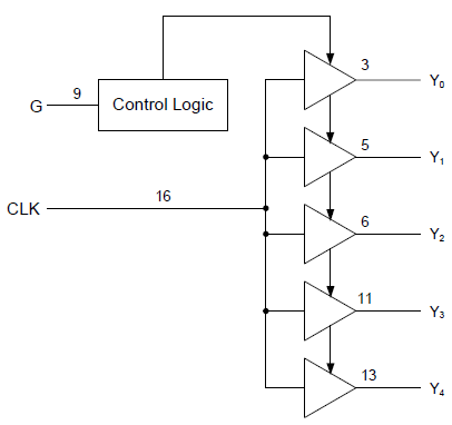
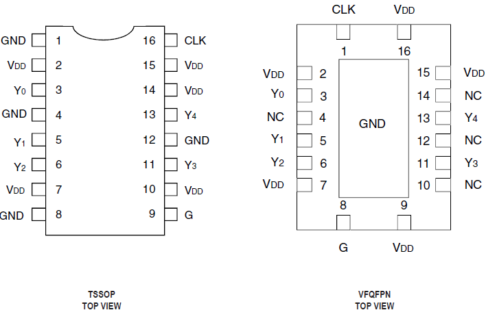
The IDT5V2305 is a high performance, low skew clock buffer that operates up to 200MHz. One bank of five outputs provides low skew copies of CLK. Through the use of control pin G, the outputs of bank Y(0:4) can be placed in a low state regardless of CLK input. The device operates in 2.5V and 3.3V environments. The built-in output enable glitch suppression ensures a synchronized output enable sequence to distribute full period clock signals. The IDT5V2305 is characterized for operation from -40°C to +85°C.
