
| CAD Model: | View CAD Model |
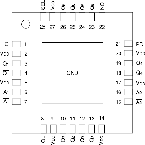
| Pkg. Type: | VFQFPN |
| Pkg. Code: | NLG28 |
| Lead Count (#): | 28 |
| Pkg. Dimensions (mm): | 6.0 x 6.0 x 0.85 |
| Pitch (mm): | 0.65 |
| Moisture Sensitivity Level (MSL) | 3 |
| Pb (Lead) Free | Yes |
| ECCN (US) | EAR99 |
| HTS (US) | 8542.39.0090 |
| Lead Count (#) | 28 |
| Carrier Type | Reel |
| Moisture Sensitivity Level (MSL) | 3 |
| Function | Buffer |
| Input Type | LVCMOS, LVDS, HSTL, LVPECL, CML |
| Output Banks (#) | 6 |
| Qty. per Reel (#) | 5000 |
| Qty. per Carrier (#) | 0 |
| Pb (Lead) Free | Yes |
| Pb Free Category | e3 Sn |
| Temp. Range (°C) | -40 to 85°C |
| Country of Assembly | MALAYSIA, TAIWAN |
| Country of Wafer Fabrication | TAIWAN, USA |
| Additive Phase Jitter Typ RMS (ps) | 0.159 |
| Core Voltage (V) | 2.5 |
| Diff. Input Signaling | 3.3, 2.5 |
| Input Freq (MHz) | 1000 |
| Inputs (#) | 2 |
| Length (mm) | 6 |
| MOQ | 5000 |
| Multiply/Divide Value | 1 |
| Operating Freq | 1000 |
| Output Freq Range (MHz) | 1000 |
| Output Signaling | LVDS |
| Output Type | LVDS |
| Output Voltage (V) | 2.5 |
| Outputs (#) | 6 |
| Package Area (mm²) | 36 |
| Pitch (mm) | 0.65 |
| Pkg. Dimensions (mm) | 6.0 x 6.0 x 0.85 |
| Pkg. Type | VFQFPN |
| Product Category | Clock Buffers & Drivers, Clock Multiplexers |
| Reel Size (in) | 13 |
| Requires Terms and Conditions | Does not require acceptance of Terms and Conditions |
| Supply Voltage (V) | 3.3 - 3.3 |
| Tape & Reel | Yes |
| Thickness (mm) | 0.85 |
| Width (mm) | 6 |
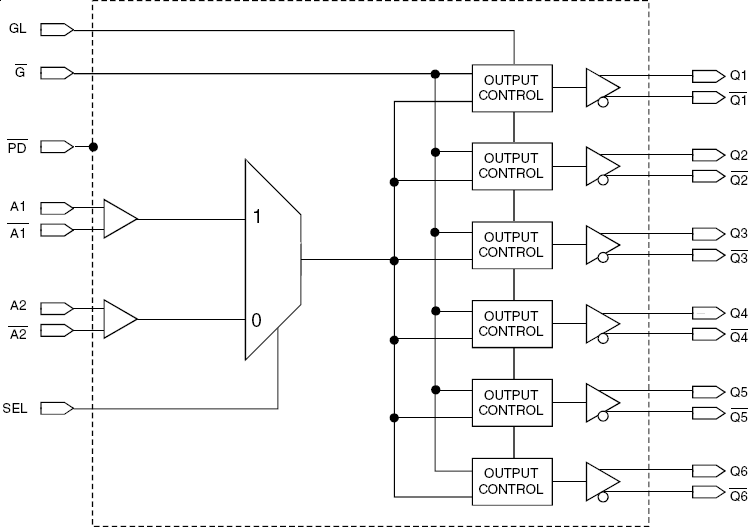
The 5T9306 2.5V differential clock buffer is a user-selectable differential input to six LVDS outputs. The fanout from a differential input to six LVDS outputs reduces loading on the preceding driver and provides an efficient clock distribution network. The 5T9306 can act as a translator from a differential HSTL, eHSTL, LVEPECL (2.5V), LVPECL (3.3V), CML, or LVDS input to LVDS outputs. A single-ended 3.3V / 2.5V LVTTL input can also be used to translate to LVDS outputs. The redundant input capability allows for an asynchronous change-over from a primary clock source to a secondary clock source. Selectable reference inputs are controlled by SEL. The 5T9306 outputs can be asynchronously enabled/disabled. When disabled, the outputs will drive to the value selected by the GL pin. Multiple power and grounds reduce noise.
