
Features
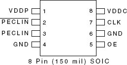
- Packaged in 8 pin SOIC (Pb-free) or die
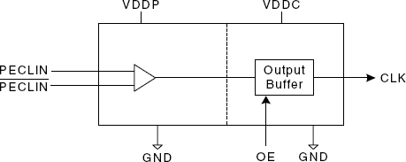
- Separate VDD supplies allow voltage translation
- Clock frequency of 0 - 250 MHz
- Duty cycle of 45/55
- Operating voltages of 2.375 to 5.5V
- Tri-state output for board level testing
- 24mA output drive capability
- Industrial temperature version available
- Advanced, low power, sub-micron CMOS process
Description
The 508 is the most cost effective way to generate a high quality, high frequency CMOS clock output from a PECL clock input. The 508 has separate VDD supplies for the PECL input buffer and the output buffer, allowing different voltages to be used. For example, the input clock could use a 3.3 V supply while the output operates from 2.5V. The device has an Output Enable pin that tri-states the clock output when the OE pin is taken low. The 508 is a member of IDT's ClockBlocksTM family.