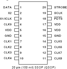

| CAD Model: | View CAD Model |
| Pkg. Type: | QSOP |
| Pkg. Code: | PCG20 |
| Lead Count (#): | 20 |
| Pkg. Dimensions (mm): | 8.7 x 3.8 x 1.47 |
| Pitch (mm): | 0.64 |
| Moisture Sensitivity Level (MSL) | 1 |
| Pb (Lead) Free | Yes |
| ECCN (US) | EAR99 |
| HTS (US) | 8542.39.0090 |
| Lead Count (#) | 20 |
| Carrier Type | Reel |
| Moisture Sensitivity Level (MSL) | 1 |
| Qty. per Reel (#) | 3000 |
| Qty. per Carrier (#) | 0 |
| Pb (Lead) Free | Yes |
| Pb Free Category | e3 Sn |
| Temp. Range (°C) | 0 to 70°C |
| Advanced Features | Programmable Clock, Reference Output |
| Core Voltage (V) | 3.3 |
| Family Name | VersaClock |
| Input Freq (MHz) | 50 |
| Input Type | Crystal, LVCMOS |
| Inputs (#) | 1 |
| Length (mm) | 8.7 |
| MOQ | 3000 |
| Output Banks (#) | 1 |
| Output Freq Range (MHz) | 0.25 - 200 |
| Output Skew (ps) | 250 |
| Output Type | LVCMOS |
| Output Voltage (V) | 3.3 |
| Outputs (#) | 9 |
| Package Area (mm²) | 33.1 |
| Period Jitter Typ P-P (ps) | 200 |
| Pitch (mm) | 0.64 |
| Pkg. Dimensions (mm) | 8.7 x 3.8 x 1.47 |
| Pkg. Type | QSOP |
| Product Category | VersaClock, Programmable Clocks |
| Prog. Clock | Yes |
| Prog. Interface | Serial |
| Reel Size (in) | 13 |
| Reference Output | Yes |
| Requires Terms and Conditions | Does not require acceptance of Terms and Conditions |
| Spread Spectrum | No |
| Tape & Reel | Yes |
| Thickness (mm) | 1.47 |
| Width (mm) | 3.8 |
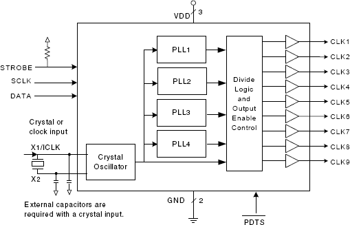
The 308 is a versatile serially programmable, quad PLL clock source. The 308 can generate any frequency from 250 kHz to 200 MHz, and up to 6 different output frequencies simultaneously. The outputs can be reprogrammed on the fly, and will lock to a new frequency in 10 ms or less. Smooth transitions (in which the clock duty cycle remains roughly 50%) are guaranteed if the output divider is not changed. The device includes a PDTS pin which tri-states the output clocks and powers down the entire chip. The 308 default for non-programmed start-up are buffered reference clock outputs on all clock output pins.
