
TOKYO, Japan, December 6, 2017 ― Renesas Electronics Corporation (TSE: 6723), a premier supplier of advanced semiconductor solutions, today announced that it has successfully confirmed large-scale memory operation in a split-gate metal-oxide nitride oxide silicon (SG-MONOS, Note 1) process using fin-shaped 3D transistors for use in microcontrollers (MCUs) with on-chip flash memory having a circuit linewidth of 16 to 14 nanometer (nm) or finer.
This result follows Renesas’ achievement in December 2016, when it announced its confirmation of operation for industry’s first SG-MONOS flash memory cells that use fin-shaped transistors. Renesas has demonstrated the operation and reliability of large-scale memory, achieving significant progress towards realizing large-capacity flash memories of more than 100 MB for use in MCUs of the 16 to 14nm and later generations.
Advances in vehicles especially the autonomous-driving vehicle and progress in the smart society connected by the Internet of Things (IoT) are accelerating, creating upsurge in demand for advanced high-performance MCUs that make use of even finer design rules to achieve higher performance and lower power consumption. To address this demand, Renesas is leading the industry by developing flash memory that can be embedded in the 16/14nm process generation, which succeeds the 40/28nm processes in which MCUs are currently either being mass produced in or are being developed for. Renesas is now working to achieve further advancement of MCUs by combining high-performance/low-power state-of-the-art logic with large-capacity/high-performance nonvolatile memory implemented with finer feature sizes.
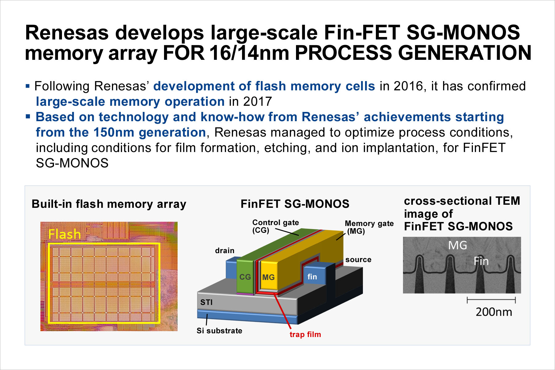
In 2016, Renesas announced the successful development of the industry's first fin-type SG-MONOS flash memory cell by applying and adopting charge trap type flash memory technology that had been used in the past. The SG-MONOS flash memory performs its data storage in a thin trap film formed on the surface of the silicon substrate, which makes it comparatively easier to deploy it in a fin structure with a three-dimensional structure. Another feature is that it is highly compatible with 16/14nm logic processes that have the same fin structure. Also, the superlative charge retention characteristics, which are a feature of charge trap type MONOS flash memory, are not degraded even when the fin structure is introduced, and Renesas has verified that the same reliability characteristics as existing devices can be achieved.
The challenge when incorporating this fin structure SG-MONOS flash memory cell in a 16/14nm generation MCU is the increase in sample-to-sample variations associated with increasing the memory capacity. Renesas succeeded in overcoming this issue and verified its operation even in a large-scale memory, which marks a significant advancement towards the achievement of high-performance, high-reliability MCUs that include an embedded flash memory system in the 100 MB class.
Renesas was able to demonstrate the following aspects of the large-scale embedded flash memory developed in this effort.
Fabrication of a memory array using a fin-structure and confirmed large-scale memory operation
In fabricating this prototype, Renesas optimized the process conditions, including the deposition, etching, and ion implantation conditions, for the fin structure. As a result, Renesas was able to prototype a memory array without increasing the number of process steps and stably acquired, even at the array level, the short channel effect suppression and the effect of reduced sample-to-sample variations expected for from the fin structure. Therefore, Renesas targets to increase capacity to the large scales of over 100 MB in a next-generation embedded flash memory.
Optimization of the write method for fin structure memory arrays
Renesas announced last year that the step pulse write method (ISSP: incremental step pulse programming) in which the write voltage is increased in steps starting at a low voltage was effective in suppressing degradation of device characteristics caused by the enhancement of electric fields at the fin tips. Now, by using this method in array operation and optimizing it, Renesas aimed at achieving both high-speed write operations and reliability. This contributed to achieving even faster write and erase operations than with earlier planar structures, and also confirmed almost no influence on write/erase speed even after the 250,000 rewrite cycles that was standard for earlier data storage flash memories.
Maintaining high-temperature data retention characteristics equivalent to existing devices at the array level
Data retention characteristics under high temperatures are critical for automotive applications. In this prototype, Renesas verified that the device maintains a guaranteed storage time after programming of at least ten years at 160°C, equivalent to earlier devices. Furthermore, this device maintains the sharp threshold voltage distribution that is a characteristic of the fin structure even after data is stored at the high temperature of 160°C at the array level, therefore maintaining the high reliability of existing devices.
The result represents a significant progress towards the achievement of high-performance MCUs that have four or more times the processing capacity of 28nm generation devices and that includes memory capacities in excess of 100 MB for the 16/14nm generation and beyond, using SG-MONOS structure flash memory.
Currently, Renesas mass produces MCUs fabricated in a 40nm generation process using SG-MONOS structure flash memory and is also developing 28nm generation MCUs. Based on the demonstration of large-scale memory operation, Renesas plans to develop 16/14nm generation MCUs with a target of 2023 for practical applications and is committed to continuing to contribute to progress in the automotive field and the achievement of a smart society.
Renesas presented the results of this research on December 5 at the International Electron Devices Meeting 2017 (IEDM 2017), which runs from December 4 to 6, 2017, in San Francisco, U.S.
(Note 1) MONOS stands for Metal-Oxide-Nitride-Oxide-Silicon. It has a structure in which each transistor (memory cell) consists of three layers—oxide, nitride, and oxide—on a silicon base, with a metal control gate at the top. Renesas has more than two decades of experience in the use of MONOS flash memory technology in chips for smart cars. Based on this track record, Renesas has successfully extended the technology by developing a split-gate (SG) structure called SG-MONOS. Embedded in Renesas MCUs the new SG-MONOS flash memory delivers high reliability, high speed, and low power consumption.
About Renesas Electronics Corporation
Renesas Electronics Corporation (TSE: 6723) delivers trusted embedded design innovation with complete semiconductor solutions that enable billions of connected, intelligent devices to enhance the way people work and live. A global leader in microcontrollers, analog, power, and SoC products, Renesas provides comprehensive solutions for a broad range of automotive, industrial, infrastructure, and IoT applications that help shape a limitless future. Learn more at renesas.com. Follow us on LinkedIn, Facebook, Twitter, and YouTube.
(Remarks) All other names of products or services mentioned in this press release are trademarks or registered trademarks of their respective owners.
The content in the press release, including, but not limited to, product prices and specifications, is based on the information as of the date indicated on the document, but may be subject to change without prior notice.