
Package Information
| CAD Model: | View CAD Model |
| Pkg. Type: | VFQFPN |
| Pkg. Code: | NLG40 |
| Lead Count (#): | 40 |
| Pkg. Dimensions (mm): | 6.0 x 6.0 x 0.9 |
| Pitch (mm): | 0.5 |
Environmental & Export Classifications
| Moisture Sensitivity Level (MSL) | 3 |
| Pb (Lead) Free | Yes |
| ECCN (US) | EAR99 |
| HTS (US) | 8542.39.0090 |
Product Attributes
| Lead Count (#) | 40 |
| Carrier Type | Tray |
| Moisture Sensitivity Level (MSL) | 3 |
| Reference Output | Yes |
| Spread Spectrum | No |
| Pb (Lead) Free | Yes |
| Pb Free Category | e3 Sn |
| Temp. Range (°C) | -40 to 85°C |
| Advanced Features | Programmable Clock, Spread Spectrum |
| C-C Jitter Max P-P (ps) | 40 |
| Core Voltage (V) | 3.3V, 2.5V |
| Divider Value | 2 |
| Family Name | UFT |
| Feedback Divider | 1 - 255 |
| Feedback Input | No |
| Input Freq (MHz) | 0.008 - 710 |
| Input Type | Crystal, LVPECL, LVDS, HSTL, HCSL |
| Inputs (#) | 3 |
| Length (mm) | 6 |
| MOQ | 490 |
| Output Banks (#) | 1 |
| Output Freq Range (MHz) | 0.98 - 1300 |
| Output Signaling | LVPECL, LVDS |
| Output Skew (ps) | 30 |
| Output Type | LVPECL, LVDS |
| Output Voltage (V) | 3.3V, 2.5V |
| Outputs (#) | 2 |
| Package Area (mm²) | 36 |
| Period Jitter Max P-P (ps) | 7.5 |
| Period Jitter Typ P-P (ps) | 4.7 |
| Phase Jitter Max RMS (ps) | 0.493 |
| Phase Jitter Typ RMS (fs) | 321 |
| Phase Jitter Typ RMS (ps) | 0.321 |
| Pitch (mm) | 0.5 |
| Pkg. Dimensions (mm) | 6.0 x 6.0 x 0.9 |
| Pkg. Type | VFQFPN |
| Product Category | FemtoClock, Low Jitter Clocks (<700 fs RMS), Programmable Clocks, Universal Frequency Translators |
| Prog. Clock | Yes |
| Prog. Interface | I2C |
| Qty. per Carrier (#) | 490 |
| Qty. per Reel (#) | 0 |
| Requires Terms and Conditions | Does not require acceptance of Terms and Conditions |
| Tape & Reel | No |
| Thickness (mm) | 0.9 |
| VCO Max Freq (MHz) | 2600 |
| VCO Min Freq (MHz) | 1995 |
| Width (mm) | 6 |
| Xtal Freq (KHz) | 16 - 40 |
| Xtal Inputs (#) | 1 |
Resources for 849N202I
Description
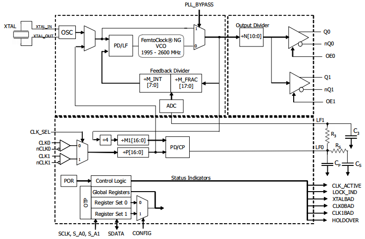
The 849N202I is a highly flexible FemtoClock® NG general purpose, low phase noise Universal Frequency Translator™ / Synthesizer with alarm and monitoring functions suitable for networking and communications applications. It is able to generate any output frequency in the 0.98MHz - 312.5MHz range and most output frequencies in the 312.5MHz - 1,300MHz range (see Table 3 for details). A wide range of input reference clocks and a range of low-cost fundamental mode crystal frequencies may be used as the source for the output frequency.
The 849N202I has three operating modes to support a very broad spectrum of applications.
To see other devices in this product family, visit the Universal Frequency Translators page.
