

| CAD Model: | View CAD Model |
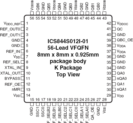
| Pkg. Type: | VFQFPN |
| Pkg. Code: | NLG56 |
| Lead Count (#): | 56 |
| Pkg. Dimensions (mm): | 8.0 x 8.0 x 0.85 |
| Pitch (mm): | 0.5 |
| Pb (Lead) Free | Yes |
| Moisture Sensitivity Level (MSL) | 3 |
| ECCN (US) | |
| HTS (US) |
| Pkg. Type | VFQFPN |
| Lead Count (#) | 56 |
| Pb (Lead) Free | Yes |
| Carrier Type | Reel |
| Advanced Features | Spread Spectrum, Reference Output |
| App Jitter Compliance | PCIe Gen1, SRIO |
| Architecture | Common |
| C-C Jitter Max P-P (ps) | 35 |
| Core Voltage (V) | 3.3 |
| Diff. Output Signaling | LVDS, LVCMOS |
| Diff. Outputs | 2 |
| Diff. Termination Resistors | 2 |
| Feedback Input | No |
| Input Freq (MHz) | 25 - 25 |
| Input Type | Crystal, LVCMOS |
| Inputs (#) | 2 |
| Length (mm) | 8 |
| MOQ | 3000 |
| Moisture Sensitivity Level (MSL) | 3 |
| Output Banks (#) | 3 |
| Output Freq Range (MHz) | 25 - 250 |
| Output Skew (ps) | 130 |
| Output Type | LVCMOS, LVDS |
| Output Voltage (V) | 3.3 |
| Outputs (#) | 12 |
| PLL | Yes |
| Package Area (mm²) | 64 |
| Pb Free Category | e3 Sn |
| Period Jitter Max P-P (ps) | 6 |
| Pitch (mm) | 0.5 |
| Pkg. Dimensions (mm) | 8.0 x 8.0 x 0.85 |
| Power Consumption Typ (mW) | 980 |
| Prog. Clock | No |
| Qty. per Carrier (#) | 0 |
| Qty. per Reel (#) | 3000 |
| Reel Size (in) | 13 |
| Reference Output | Yes |
| Requires Terms and Conditions | Does not require acceptance of Terms and Conditions |
| Spread Spectrum | Yes |
| Supply Voltage (V) | 3.3 - 3.3 |
| Tape & Reel | Yes |
| Temp. Range (°C) | -40 to 85°C |
| Thickness (mm) | 0.85 |
| Width (mm) | 8 |
| Xtal Freq (MHz) | 25 - 25 |
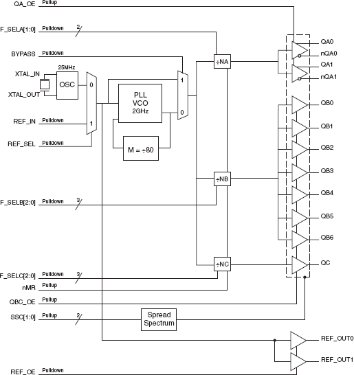
The 844S012I-01 is an optimized PCIe, sRIO and Gigabit Ethernet Frequency Synthesizer. The 844S012I-01 uses a 25MHz parallel resonant crystal to generate 33.33MHz - 200MHz clock signals, replacing solutions requiring multiple oscillator and fanout buffer solution. The device supports ±0.25% center-spread, and -0.6% down-spread clocking with two spread select pins (SSC[1:0]). The VCO operates at frequency of 2GHz. The device has three output banks: Bank A with two LVDS outputs, 100MHz – 250MHz; Bank B with seven 33.33MHz – 200MHz LVCMOS/ LVTTL outputs; and Bank C with one 33.33MHz – 200MHz LVCMOS/LVTTL output.
All Banks A, B and C have their own dedicated frequency select pins and can be independently set for the frequencies mentioned above. The low jitter characteristic of the 844S012I-01 makes it an ideal clock source for PCIe, sRIO and Gigabit Ethernet applications. Designed for networking and industrial applications, the 844S012I-01 can also drive the high-speed clock inputs of communication processors, DSPs, switches and bridges. The 843241I-04 is a Serial ATA (SATA)/Serial Attached SCSI (SAS) Clock Generator and a member of the HiPerClocksTM family of high performance devices from IDT. For SATA/SAS applications, a 25MHz crystal is used to produce 150MHz. The 843241I-04 is packaged in a small 8-pin TSSOP, making it ideal for use in systems with limited board space.
