
| CAD Model: | View CAD Model |
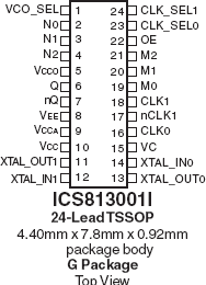
| Pkg. Type: | TSSOP |
| Pkg. Code: | PGG24 |
| Lead Count (#): | 24 |
| Pkg. Dimensions (mm): | 7.8 x 4.4 x 1.0 |
| Pitch (mm): | 0.65 |
| Moisture Sensitivity Level (MSL) | 1 |
| Pb (Lead) Free | Yes |
| ECCN (US) | EAR99 |
| HTS (US) | 8542.39.0090 |
| Lead Count (#) | 24 |
| Carrier Type | Tube |
| Moisture Sensitivity Level (MSL) | 1 |
| Qty. per Reel (#) | 0 |
| Qty. per Carrier (#) | 62 |
| Pb (Lead) Free | Yes |
| Pb Free Category | e3 Sn |
| Temp. Range (°C) | -40 to 85°C |
| Core Voltage (V) | 3.3 |
| Feedback Input | No |
| Input Freq (MHz) | 14 - 24 |
| Input Type | Crystal, LVCMOS, LVPECL, LVDS, LVHSTL, SSTL, HCSL |
| Inputs (#) | 4 |
| Length (mm) | 7.8 |
| MOQ | 62 |
| Output Banks (#) | 1 |
| Output Freq Range (MHz) | 40.83 - 640 |
| Output Type | LVPECL |
| Output Voltage (V) | 3.3V, 2.5V |
| Outputs (#) | 1 |
| Package Area (mm²) | 34.3 |
| Phase Jitter Typ RMS (ps) | 0.84 |
| Pitch (mm) | 0.65 |
| Pkg. Dimensions (mm) | 7.8 x 4.4 x 1.0 |
| Pkg. Type | TSSOP |
| Product Category | FemtoClock, Low Jitter Clocks (<700 fs RMS) |
| Prog. Clock | No |
| Reference Output | No |
| Requires Terms and Conditions | Does not require acceptance of Terms and Conditions |
| Spread Spectrum | No |
| Tape & Reel | No |
| Thickness (mm) | 1 |
| Width (mm) | 4.4 |
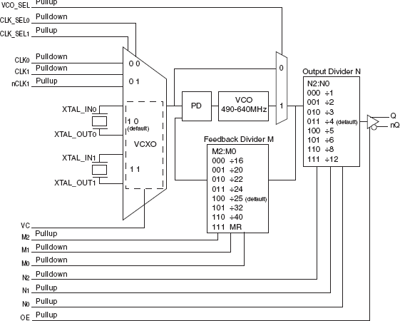
The 813001I is a dual VCXO + FemtoClock® multiplier designed for use in discrete PLL loops. Two selectable external VCXO crystals allow the device to be used in multi-rate applications, where a given line card can be switched, for example, between 1Gb Ethernet (125MHz system reference clock) and 1Gb Fibre Channel (106.25MHz system reference clock) modes. Of course, a multitude of other applications are also possible such as switching between 74.25MHz and 74.175824MHz for HDTV, switching between SONET, FEC, and non-FEC rates, etc. The 813001I is a two-stage device – a VCXO followed by a FemtoClock PLL. The FemtoClock PLL can multiply the crystal frequency of the VCXO to provide an output frequency range of 40.83MHz to 640MHz, with a random RMS phase jitter of less than 1ps (12kHz – 20MHz). This phase jitter performance meets the requirements of 1Gb/ 10Gb Ethernet, 1Gb, 2Gb, 4Gb, and 10Gb Fibre Channel, and SONET up to OC48. The FemtoClock PLL can also be bypassed if frequency multiplication is not required. For testing/debuging purposes, de-assertion of the output enable pin will place both Q and nQ in a high impedance state.