Features
- Generates up to four independent output frequencies with a total of 7 differential outputs and one reference LVCMOS output
- Supports multiple differential output I/O standards:
- Three universal output pairs with each configurable as one differential output pair (LVDS, LVPECL, or regular HCSL) or two LVCMOS outputs. The frequency of each output pair can be individually programmed
- Four copies of Low Power HCSL (LP-HCSL) outputs
- Meets PCIe® Gen 1/2/3, USB 3.0, 1/10 GbE clock requirements
- <0.7ps RMS typical phase jitter on outputs
- Four fractional output dividers (FODs)
- Independent spread spectrum capability from each fractional output divider
- Stores 4 different configurations in OTP non-volatile memory
- Input frequency ranges up to 200MHz
- Output frequency ranges up to 350MHz
- Programmable loop bandwidth and crystal load capacitance
- 1.8V/2.5V/3.3V core and output voltages
- Supported by the Timing Commander™ software tool


Description
The 5P49V5907 is a programmable clock generator intended for high-performance consumer, networking, industrial, computing, and data communications applications. Configurations may be stored in on-chip One-Time Programmable (OTP) memory or changed using the I2C interface. This is Renesas' fifth generation of programmable clock technology (VersaClock® 5). The frequencies are generated from a single reference clock or crystal.
Two select pins allow up to four different configurations to be programmed and accessible using processor GPIOs or bootstrapping. The different selections may be used for different operating modes (full function, partial function, partial power down), regional standards (US, Japan, Europe), or system production margin testing. The device may be configured to use one of two I2C addresses to allow multiple devices to be used in a system. The device is packaged in a 40-pin 5mm x 5mm VFQFPN (NDG40), with an industrial operating temperature of -40 °C to +85 °C.
Applications
- Ethernet switch/router
- PCI Express 1.0/2.0/3.0
- Broadcast video/audio timing
- Multi-function printer
- Processor and FPGA clocking
- Any-frequency clock conversion
- MSAN/DSLAM/PON
- Fiber Channel, SAN
- Telecom line cards
- 1GbE and 10GbE
| Part Number | Status | Samples | Stock | Package | Budgetary Price (USD) | Lead Count (#) | Carrier Type | Moisture Sensitivity Level (MSL) | Qty. per Reel (#) | Qty. per Carrier (#) | Pb (Lead) Free | Pb Free Category | Temp. Range (°C) | Country of Assembly | Country of Wafer Fabrication |
|---|---|---|---|---|---|---|---|---|---|---|---|---|---|---|---|
| 5P49V5907A000NDGI | NRND | Available | Out of Stock | VFQFPN | 40# | Tray | 3 | 0 | 490# | Yes | e3 Sn | -40 to 85°C | |||
| 5P49V5907A000NDGI8 | NRND | N/A | Out of Stock | VFQFPN | 40# | Reel | 3 | 2500# | 0 | Yes | e3 Sn | -40 to 85°C | |||
| 5P49V5907B000NDGI | NRND | Available | In Stock | VFQFPN | 1ku | $5.78 | 40# | Tray | 3 | 0 | 490# | Yes | e3 Sn | -40 to 85°C | TAIWAN | SINGAPORE, TAIWAN |
| 5P49V5907B000NDGI8 | NRND | N/A | Out of Stock | VFQFPN | 1ku | $5.78 | 40# | Reel | 3 | 2500# | 0 | Yes | e3 Sn | -40 to 85°C | TAIWAN | SINGAPORE, TAIWAN |
Filters
Applied Filters
- Application NotePDF 1.09 MB R31AN0026EU0102 Rev.1.02 Sep 06, 2025
- Application NotePDF 187 KB R31AN0065EU0101 Rev.1.01 Nov 14, 2023
- Application NotePDF 348 KB R31AN0040EU0100 Rev.1.00 Mar 10, 2023
- Manual - Development ToolsPDF 1.25 MB 7WDXRDKU4E7E-5-57450 Feb 02, 2023
- Product Change NoticePDF 726 KB Aug 20, 2021
- Application NotePDF 486 KB 7WDXRDKU4E7E-5-63374 Nov 01, 2018
- Application NotePDF 717 KB 7WDXRDKU4E7E-5-61645 May 11, 2017
- Application NotePDF 307 KB 7WDXRDKU4E7E-5-59989 Mar 10, 2016
- Application NotePDF 144 KB 7WDXRDKU4E7E-5-59783 Dec 03, 2015
- Manual - SoftwarePDF 2.04 MB 7WDXRDKU4E7E-5-57026 Oct 07, 2015
- Application NotePDF 235 KB 7WDXRDKU4E7E-5-58851 Apr 08, 2015
- Application NotePDF 176 KB 7WDXRDKU4E7E-5-57449 Jun 26, 2014
Recommended Documents (1)
Datasheets (1)
- Manual - Development ToolsPDF 1.25 MB 7WDXRDKU4E7E-5-57450 Feb 02, 2023
- Manual - SoftwarePDF 2.04 MB 7WDXRDKU4E7E-5-57026 Oct 07, 2015
Manuals & Guides (2)
- Application NotePDF 1.09 MB R31AN0026EU0102 Rev.1.02 Sep 06, 2025
- Application NotePDF 187 KB R31AN0065EU0101 Rev.1.01 Nov 14, 2023
- Application NotePDF 348 KB R31AN0040EU0100 Rev.1.00 Mar 10, 2023
- Application NotePDF 486 KB 7WDXRDKU4E7E-5-63374 Nov 01, 2018
Application Notes & White Papers (16)
- Product Change NoticePDF 726 KB Aug 20, 2021
- Product Change NoticePDF 344 KB 7WDXRDKU4E7E-5-59950 Feb 20, 2016
- Product Change NoticePDF 243 KB 7WDXRDKU4E7E-5-59639 Oct 29, 2015
Product Notices (PCN, EOL, etc) (3)
No Results Found.
Make sure all keywords are spelled correctly.
Try fewer, different, or more general terms to vary your search.
If you have filters applied, consider deselecting some to broaden your results.
- Search our extensive knowledgebase, designed to help customers with their FAQs.
- Get help from our expert Renesas technical staff and community on our support forums.
- Product BriefPDF 1.01 MB 7WDXRDKU4E7E-6-10379 Jun 29, 2015
Marketing Collateral (1)
No Results Found.
Make sure all keywords are spelled correctly.
Try fewer, different, or more general terms to vary your search.
If you have filters applied, consider deselecting some to broaden your results.
- Search our extensive knowledgebase, designed to help customers with their FAQs.
- Get help from our expert Renesas technical staff and community on our support forums.
Renesas Boards & Kits
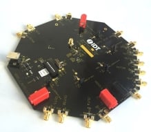
Evaluation Board for 5P49V5907 VersaClock 5
This is the evaluation board for the Renesas 5P49V5907 programmable clock generator. With RMS phase jitter less than 0.75 picoseconds over the full 12kHz to 20MHz integration range, the device meets the stringent jitter requirements of PCI Express® Gen 1/2/3, USB 3.0, and 1G/10G Ethernet.... Read More
Filters
Applied Filters
Software & Tools
Filter by Type
Filter by Provider
Sample Code
Filter by Application
Filter by Function
Filter by Compiler
Filter by IDE
Simulation Models
Partner Solutions
- Software & Tools - Other
- Software & Tools - Software
- Code GeneratorTiming Commander™ is an innovative Windows™-based software platform enabling system design engineers to configure, program, and monitor sophisticated timing devices with an intuitive and flexible graphical user interface (GUI).
No Results Found.
Make sure all keywords are spelled correctly.
Try fewer, different, or more general terms to vary your search.
If you have filters applied, consider deselecting some to broaden your results.
- Search our extensive knowledgebase, designed to help customers with their FAQs.
- Get help from our expert Renesas technical staff and community on our support forums.
- Software & Tools - Other
- Software & Tools - Software
- Code GeneratorTiming Commander™ is an innovative Windows™-based software platform enabling system design engineers to configure, program, and monitor sophisticated timing devices with an intuitive and flexible graphical user interface (GUI).
Software & Tools (3)
No Results Found.
Make sure all keywords are spelled correctly.
Try fewer, different, or more general terms to vary your search.
If you have filters applied, consider deselecting some to broaden your results.
- Search our extensive knowledgebase, designed to help customers with their FAQs.
- Get help from our expert Renesas technical staff and community on our support forums.
Simulation Models (1)
No Results Found.
Make sure all keywords are spelled correctly.
Try fewer, different, or more general terms to vary your search.
If you have filters applied, consider deselecting some to broaden your results.
- Search our extensive knowledgebase, designed to help customers with their FAQs.
- Get help from our expert Renesas technical staff and community on our support forums.
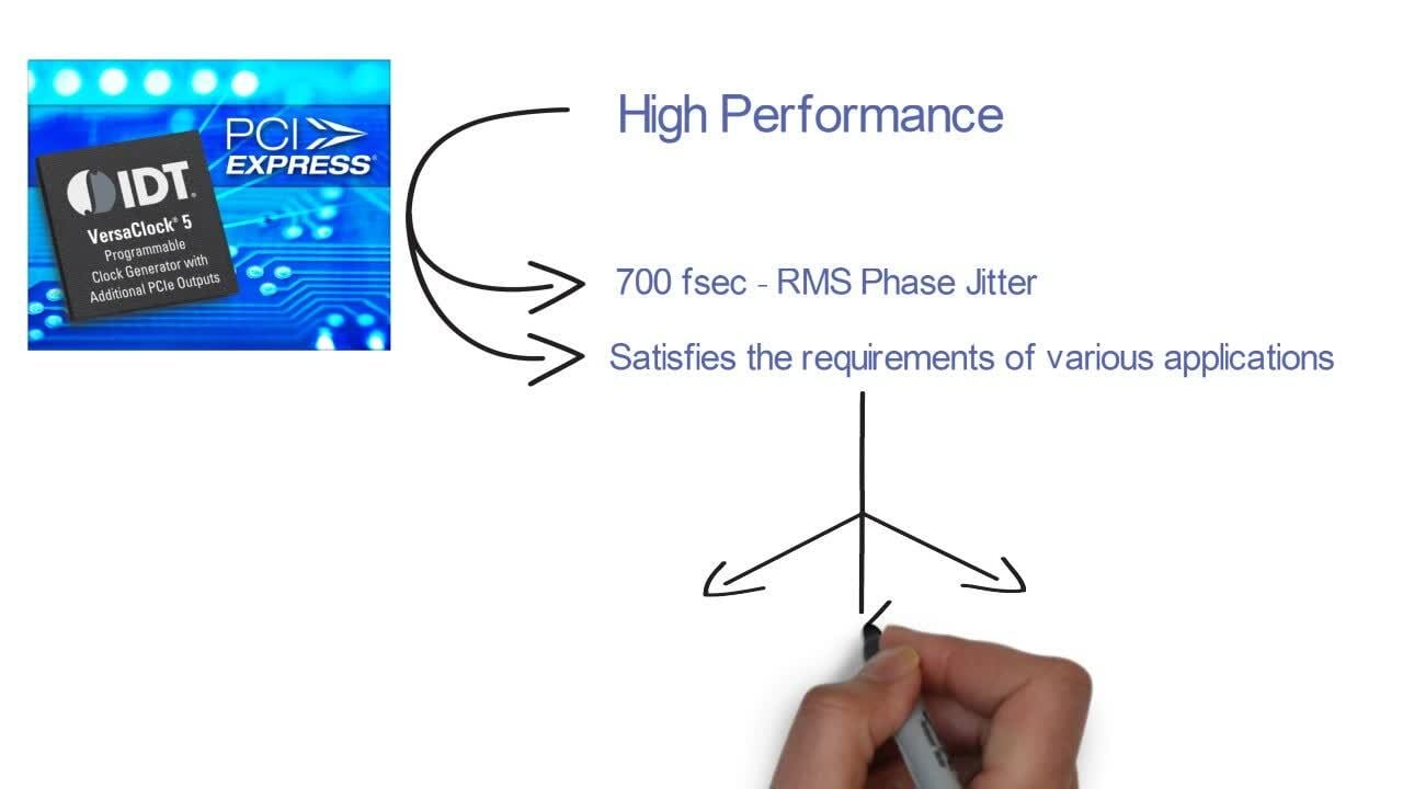
This video provides an overview of IDT's programmable clock generators 5P49V5907 and 5P49V5908 featuring the fifth generation of programmable clock technology (VersaClock® 5). With additional outputs supporting PCI Express® timing, these devices present a blend of low power, flexibility, and high performance suitable for a wide range of applications including performance consumer, networking, industrial, computing, and data communications. For more information, visit the Programmable Clocks page.
Lab demonstration and clock jitter measurement showing VersaClock 5. The frequency analyzer shows phase jitter at approximately 575 picoseconds RMS. Presented by Baljit Chandhoke, product manager at IDT. For more information visit the Programmable Clocks page.
This video will show you how to program VersaClock® 5 Low Power Programmable Clock Generator.
Description
IDT's innovative support tool, Timing Commander™, expedites development cycles by empowering customers to program sophisticated timing devices with an intuitive and flexible Graphical User Interface. IDT's Timing Commander is a Windows™-based platform designed to serve user-friendly configuration interfaces, known as personalities, for various IDT products and product families. With a few simple clicks, the user is presented with a comprehensive, interactive block diagram offering the ability to modify desired input values, output values, and other configuration settings. The software automatically makes calculations, reports status monitors, and prepares register settings without the need to reference a datasheet. The tool also automatically loads the configuration settings over USB to an IDT evaluation board for immediate application in the circuit. Once the device has been configured and tuned for optimal system performance, the configuration file can be saved for factory-level programming before shipment. For more information about Timing Commander, visit our Timing Commander page.
Resources
IDT (acquired by Renesas) engineer provides a brief tutorial describing the main differences between standard HCSL and low-power HCSL (LP-HCSL).
Presented by Ron Wade, PCI Express timing expert.
News & Blog Posts

Support Communities


