
Features
- One 3.3V or 2.5V LVPECL output pair
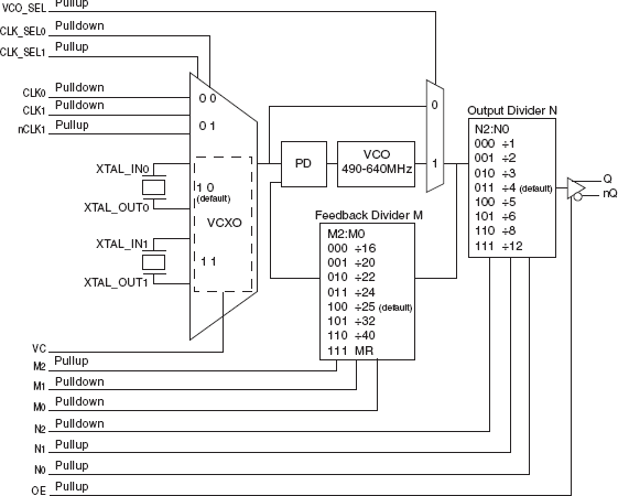
- Two selectable crystal oscillator interfaces for the VCXO, one differential clock or one LVCMOS/LVTTL clock inputs
- CLK1/nCLK1 supports the following input types: LVPECL, LVDS, LVHSTL, SSTL, HCSL
- Crystal operating frequency range: 14MHz - 24MHz
- VCO range: 490MHz - 640MHz
- Output frequency range: 40.83MHz - 640MHz
- VCXO pull range: ±100ppm (typical)
- Supports the following applications (among others): SONET, Ethernet, Fibre Channel, HDTV, MPEG
- RMS phase jitter @ 622.08MHz (12kHz - 20MHz): 0.84 (typical)
- Supply voltage modes: VCC/VCCO 3.3V/3.3V 3.3V/2.5V 2.5V/2.5V
- -40°C to 85°C ambient operating temperature
- Available in RoHS/Lead-Free compliant package
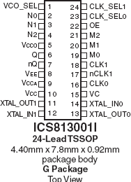
Description
The 813001I is a dual VCXO + FemtoClock® multiplier designed for use in discrete PLL loops. Two selectable external VCXO crystals allow the device to be used in multi-rate applications, where a given line card can be switched, for example, between 1Gb Ethernet (125MHz system reference clock) and 1Gb Fibre Channel (106.25MHz system reference clock) modes. Of course, a multitude of other applications are also possible such as switching between 74.25MHz and 74.175824MHz for HDTV, switching between SONET, FEC, and non-FEC rates, etc. The 813001I is a two-stage device – a VCXO followed by a FemtoClock PLL. The FemtoClock PLL can multiply the crystal frequency of the VCXO to provide an output frequency range of 40.83MHz to 640MHz, with a random RMS phase jitter of less than 1ps (12kHz – 20MHz). This phase jitter performance meets the requirements of 1Gb/ 10Gb Ethernet, 1Gb, 2Gb, 4Gb, and 10Gb Fibre Channel, and SONET up to OC48. The FemtoClock PLL can also be bypassed if frequency multiplication is not required. For testing/debuging purposes, de-assertion of the output enable pin will place both Q and nQ in a high impedance state.