
Features
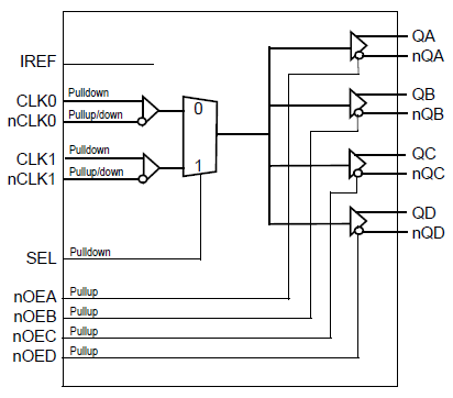
- 2:1 differential clock/data multiplexer with fanout
- Two selectable, differential inputs
- Each differential input pair can accept the following levels: HCSL, LVDS, LVPECL
- Four differential HCSL outputs
- Maximum input/output clock frequency: 350MHz
- Maximum input/output data rate: 700Mb/s (NRZ)
- LVCMOS interface levels for all control inputs
- PCI Express Gen 1,2,3 jitter compliant
- Input skew: 165ps (maximum)
- Output skew: 175ps (maximum)
- Part-to-part skew: 450ps (maximum)
- Full 3.3V supply voltage
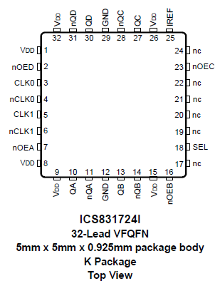
- Available in lead-free (RoHS 6) package
- -40°C to 85°C ambient operating temperature
Description
The 831724I is a high-performance, differential HCSL clock/data multiplexer and fanout buffer. The device is designed for the multiplexing and fanout of high-frequency clock and data signals. The device has two differential, selectable clock/data inputs. The selected input signal is distributed to four low-skew differential HCSL outputs. Each input pair accepts HCSL, LVDS, LVPECL and SSTL levels. The 831724I is characterized to operate from a 3.3V power supply. Guaranteed input, output-to-output and part-to-part skew characteristics make the 831724I ideal for those clock and data distribution applications demanding well-defined performance and repeatability. The 831724I supports the clock multiplexing and distribution of PCI Express (2.5 Gb/s) and Gen 2 (5 Gb/s) clock signals. The device is a member of the family of High Performance Clock Solutions from IDT.
| Part Number | Status | Samples | Stock | Package | Lead Count (#) | Carrier Type | Moisture Sensitivity Level (MSL) | Qty. per Reel (#) | Qty. per Carrier (#) | Pb (Lead) Free | Pb Free Category | Temp. Range (°C) |
|---|---|---|---|---|---|---|---|---|---|---|---|---|
| 831724AKILF | Obsolete | N/A | Out of Stock | VFQFPN | 32# | Tray | 3 | 0 | 490# | Yes | e3 Sn | -40 to 85°C |
| 831724AKILFT | Obsolete | N/A | Out of Stock | VFQFPN | 32# | Reel | 3 | 2500# | 0 | Yes | e3 Sn | -40 to 85°C |
Filters
Applied Filters
- Application NotePDF 170 KB 7WDXRDKU4E7E-5-57318 May 13, 2014
- Application NotePDF 495 KB 7WDXRDKU4E7E-5-57312 May 12, 2014
- Application NotePDF 442 KB 7WDXRDKU4E7E-5-57298 May 08, 2014
- Application NotePDF 120 KB 7WDXRDKU4E7E-5-57289 May 06, 2014
- Application NotePDF 160 KB 7WDXRDKU4E7E-5-57287 May 06, 2014
- Application NotePDF 180 KB 7WDXRDKU4E7E-5-57283 May 06, 2014
- Product Change NoticePDF 983 KB Jun 25, 2019
- Product Change NoticePDF 583 KB 7WDXRDKU4E7E-5-61343 Dec 20, 2016
Recommended Documents (1)
Datasheets (1)
No Results Found.
Make sure all keywords are spelled correctly.
Try fewer, different, or more general terms to vary your search.
If you have filters applied, consider deselecting some to broaden your results.
- Search our extensive knowledgebase, designed to help customers with their FAQs.
- Get help from our expert Renesas technical staff and community on our support forums.
- Application NotePDF 1.99 MB 7WDXRDKU4E7E-5-57242 Mar 01, 2022
- Application NotePDF 170 KB 7WDXRDKU4E7E-5-57318 May 13, 2014
- Application NotePDF 495 KB 7WDXRDKU4E7E-5-57312 May 12, 2014View More (11)
Application Notes & White Papers (11)
- Product Change NoticePDF 983 KB Jun 25, 2019
- Product Change NoticePDF 583 KB 7WDXRDKU4E7E-5-61343 Dec 20, 2016
- Product Change NoticePDF 596 KB 7WDXRDKU4E7E-5-59884 Jan 28, 2016View More (6)
Product Notices (PCN, EOL, etc) (6)
No Results Found.
Make sure all keywords are spelled correctly.
Try fewer, different, or more general terms to vary your search.
If you have filters applied, consider deselecting some to broaden your results.
- Search our extensive knowledgebase, designed to help customers with their FAQs.
- Get help from our expert Renesas technical staff and community on our support forums.
No Results Found.
Make sure all keywords are spelled correctly.
Try fewer, different, or more general terms to vary your search.
If you have filters applied, consider deselecting some to broaden your results.
- Search our extensive knowledgebase, designed to help customers with their FAQs.
- Get help from our expert Renesas technical staff and community on our support forums.
No Results Found.
Make sure all keywords are spelled correctly.
Try fewer, different, or more general terms to vary your search.
If you have filters applied, consider deselecting some to broaden your results.
- Search our extensive knowledgebase, designed to help customers with their FAQs.
- Get help from our expert Renesas technical staff and community on our support forums.
No Results Found.
Make sure all keywords are spelled correctly.
Try fewer, different, or more general terms to vary your search.
If you have filters applied, consider deselecting some to broaden your results.
- Search our extensive knowledgebase, designed to help customers with their FAQs.
- Get help from our expert Renesas technical staff and community on our support forums.
No Results Found.
Make sure all keywords are spelled correctly.
Try fewer, different, or more general terms to vary your search.
If you have filters applied, consider deselecting some to broaden your results.
- Search our extensive knowledgebase, designed to help customers with their FAQs.
- Get help from our expert Renesas technical staff and community on our support forums.
No Results Found.
Make sure all keywords are spelled correctly.
Try fewer, different, or more general terms to vary your search.
If you have filters applied, consider deselecting some to broaden your results.
- Search our extensive knowledgebase, designed to help customers with their FAQs.
- Get help from our expert Renesas technical staff and community on our support forums.
Marketing Collateral (1)
No Results Found.
Make sure all keywords are spelled correctly.
Try fewer, different, or more general terms to vary your search.
If you have filters applied, consider deselecting some to broaden your results.
- Search our extensive knowledgebase, designed to help customers with their FAQs.
- Get help from our expert Renesas technical staff and community on our support forums.
No Results Found.
Make sure all keywords are spelled correctly.
Try fewer, different, or more general terms to vary your search.
If you have filters applied, consider deselecting some to broaden your results.
- Search our extensive knowledgebase, designed to help customers with their FAQs.
- Get help from our expert Renesas technical staff and community on our support forums.
No Results Found.
Make sure all keywords are spelled correctly.
Try fewer, different, or more general terms to vary your search.
If you have filters applied, consider deselecting some to broaden your results.
- Search our extensive knowledgebase, designed to help customers with their FAQs.
- Get help from our expert Renesas technical staff and community on our support forums.
Filters
Applied Filters
Software & Tools
Filter by Type
Filter by Provider
Sample Code
Filter by Application
Filter by Function
Filter by Compiler
Filter by IDE
Simulation Models
Partner Solutions
No Results Found.
Make sure all keywords are spelled correctly.
Try fewer, different, or more general terms to vary your search.
If you have filters applied, consider deselecting some to broaden your results.
- Search our extensive knowledgebase, designed to help customers with their FAQs.
- Get help from our expert Renesas technical staff and community on our support forums.
No Results Found.
Make sure all keywords are spelled correctly.
Try fewer, different, or more general terms to vary your search.
If you have filters applied, consider deselecting some to broaden your results.
- Search our extensive knowledgebase, designed to help customers with their FAQs.
- Get help from our expert Renesas technical staff and community on our support forums.
No Results Found.
Make sure all keywords are spelled correctly.
Try fewer, different, or more general terms to vary your search.
If you have filters applied, consider deselecting some to broaden your results.
- Search our extensive knowledgebase, designed to help customers with their FAQs.
- Get help from our expert Renesas technical staff and community on our support forums.
Simulation Models (1)
No Results Found.
Make sure all keywords are spelled correctly.
Try fewer, different, or more general terms to vary your search.
If you have filters applied, consider deselecting some to broaden your results.
- Search our extensive knowledgebase, designed to help customers with their FAQs.
- Get help from our expert Renesas technical staff and community on our support forums.

Support Communities


