
Features
- 8 - 0.7 V current-mode differential output pairs
- Supports zero delay buffer mode and fanout mode
- Bandwidth programming available
- Spread spectrum modulation tolerant, 0 to -0.5% down spread and +/- 0.25% center spread.
- Supports undriven differential outputs in PD# and SRC_STOP# modes for power management.
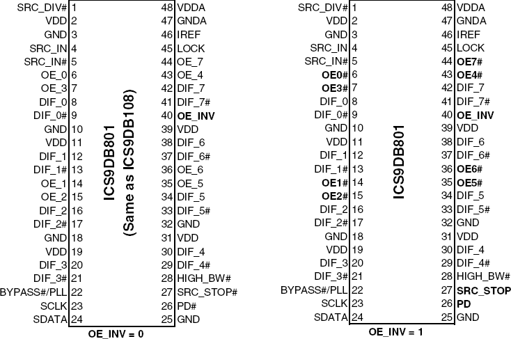
- Supports polarity inversion to the output enables, SRC_STOP and PD.
- Outputs cycle-cycle jitter < 50 ps
- Outputs skew: 50 ps
- 50 - 200 MHz operation
- Extended frequency range in bypass mode to 400 MHz
- PCI Express® Gen I compliant
- Real time PLL lock detect output pin
- 48-pin SSOP/TSSOP package
- Available in RoHS compliant packaging
Description
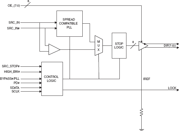
The 9DB801C is a DB800 Version 2.0 Yellow Cover part with PCI Express® support. It can be used in PC or embedded systems to provide outputs that have low cycle-to-cycle jitter (50 ps), low output-to-output skew (100 ps), and are PCI Express® gen 1 compliant. The 9DB801C supports a 1 to 8 output configuration, taking a spread or non spread differential HCSL input from a CK410(B) main clock such as 954101 and 932S401, or any other differential HCSL pair. 9DB801C can generate HCSL or LVDS outputs from 50 to 200 MHz in PLL mode or 0 to 400 MHz in bypass mode. There are two de-jittering modes available selectable through the HIGH_BW# input pin, high bandwidth mode provides de-jittering for spread inputs and low bandwidth mode provides extra de-jittering for non-spread inputs. The SRC_STOP#, PD#, and individual OE# real-time input pins provide completely programmable power management control.