Features
- Two Synchronous-Rectified Buck Controllers
- Voltage Mode Control
- VIN Range up to 12V
- VOUT Range from 0.6V to 6V
- 12V LGATE Drivers; up to 12V Boot Strap for UGATE
- Switcher References
- 0.6V Reference for OUT1
- 3.3V Reference Output for OUT2
- External Reference Input for OUT2
- Buffered VTT Reference Output
- Switcher Clocking
- Phase Options for Optimal Clock Relationship
- Resistor-Selectable Switching Frequency (300kHz default; Resistor to Ground for 300kHz to 1MHz range)
- Synchronization-Capable Switching Frequency (Connect FS_SYNC to Separate Regulator)
- Single Linear Controller
- Drives N-Channel MOSFET
- 0.6V Reference
- VIN Range up to 12V
- VOUT Range from 0.6V to 3.3V
- 12V and 5V Supplies Required (but optional shunt regulator can generate VCC = 5.8V from 12V)
- Three Independent Soft-Start/Enable Pins
- Gang Together or Control Independently
- PGOOD Output Indicates All Outputs Available
- Thermally Enhanced QFN or TSSOP Package
- QFN Package:
- Compliant to JEDEC PUB95 MO-220 QFN - Quad Flat No Leads - Package Outline
- Near Chip Scale Package footprint, which improves PCB efficiency and has a thinner profile
- Pb-Free Plus Anneal Available (RoHS Compliant)
Description
Support is limited to customers who have already adopted these products.
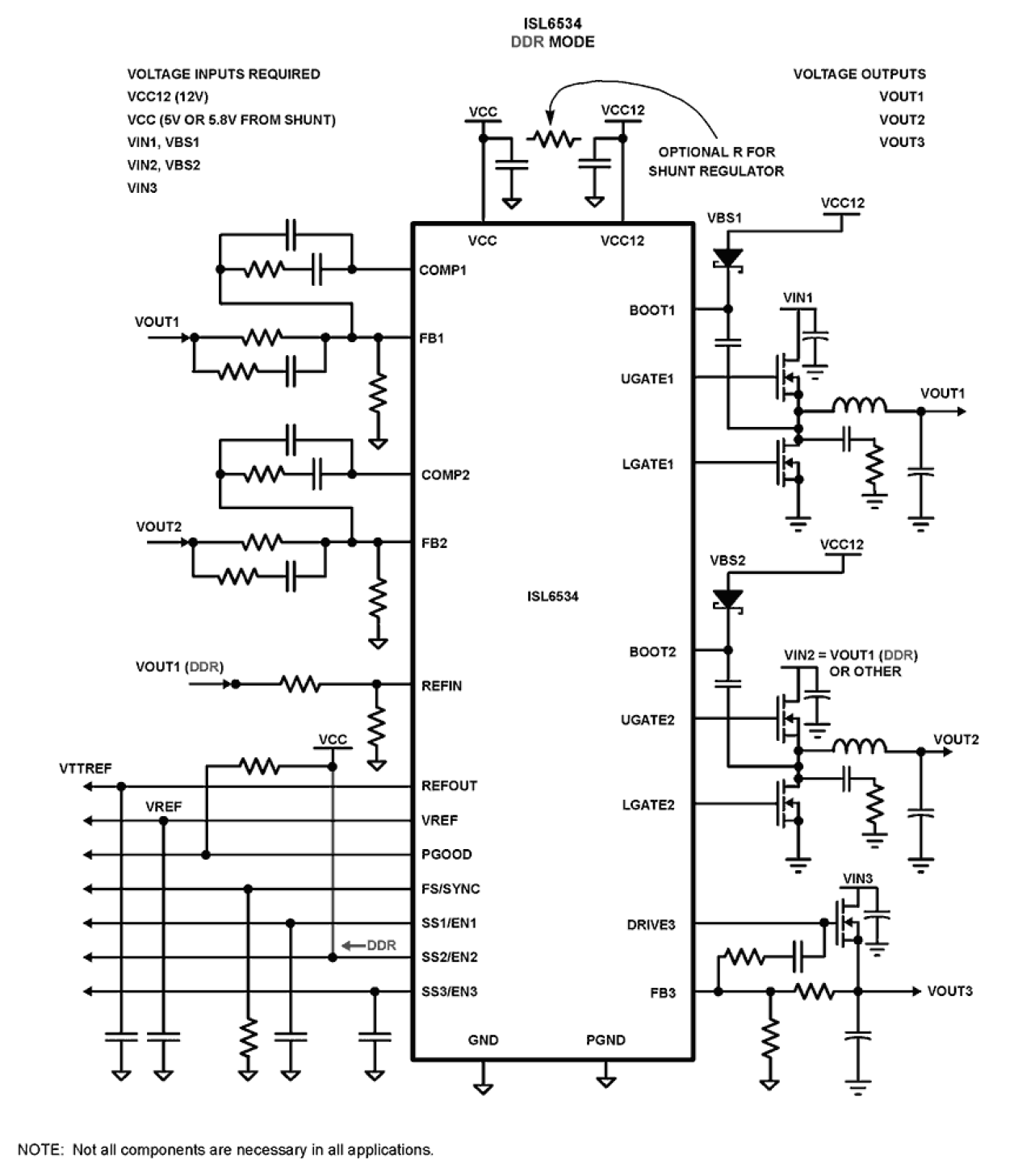
The ISL6534 is a versatile triple regulator that has two independent synchronous-rectified buck controllers with integrated 12V gate drivers (OUT1 and OUT2) and a linear controller (OUT3) to offer precision regulation of up to three voltage rails. An optional shunt regulator allows 12V only operation, when a 5V supply is not available. Each controller has independent soft-start and enable functions combined on a single pin. A capacitor from each SS/EN pin to ground sets the soft-start time, and pulling SS/EN below 1.0V disables the controller. The SS/EN pins can be controlled independently or they can be ganged together to provide complete control of start-up coordination. The PGOOD function indicates when all regulators have completed their soft-start and provides an indication of shortcircuit conditions on either switching regulator. There are two ways to control the switching frequency of the PWM regulators. The default switching frequency is 300kHz (FS_SYNC to ground). A resistor from FS_SYNC to ground increases the switching frequency (up to 1MHz). Connecting the gate signal from another PWM IC synchronizes the ISL6534 switchers to the frequency of the other controller. This allows independent regulators operating at a common frequency to avoid low-frequency beats. The gate drivers for DDR mode can be staggered by 90° in order to minimize cross-conduction. Switcher OUT1 has an internal reference for regulating any voltage down to 0.6V. OUT2 has current sinking capability and an external reference input allowing convenient connection to OUT1 through a resistor divider for DDRAM applications. The 3.3V reference pin provides the option for independent regulation of OUT2. The linear controller drives an external N-Channel MOSFET, making the ISL6534 one of the most versatile regulators available.
Applied Filters:

