Features
- 1.8V operation; reduced power consumption
- OE# pins; support DIF power management
- LP-HCSL differential clock outputs; reduced power and board space
- Programmable slew rate for each output; allows tuning for various line lengths
- Programmable output amplitude; allows tuning for various application environments
- DIF outputs are blocked until PLL is locked; clean system start-up
- Selectable 0%, -0.25%, or -0.5% spread on DIF outputs; reduces EMI
- External 25MHz crystal; supports tight ppm with 0ppm synthesis error
- Configuration can be accomplished with strapping pins; SMBus interface is not required for device control
- 3.3V tolerant SMBus interface works with legacy controllers
- Space-saving 5mm x 5mm 32-VFQFPN; minimal board space
- Selectable SMBus addresses; multiple devices can easily share an SMBus segment
Description
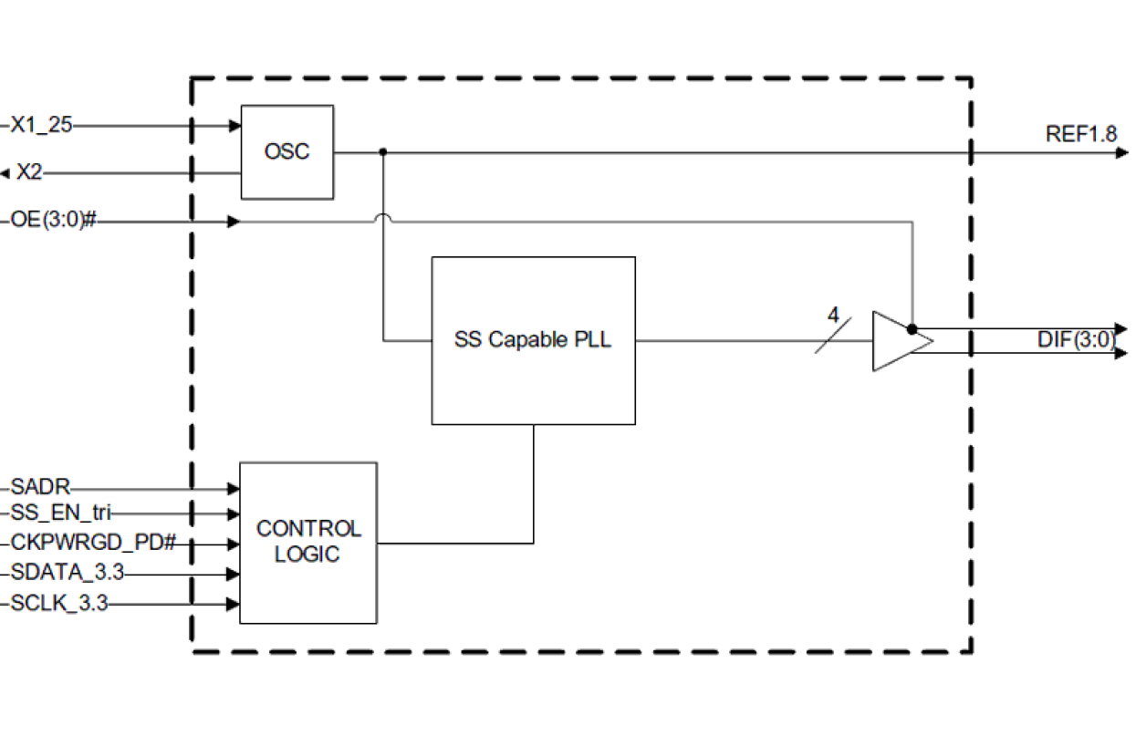
The 9FGV0431 is a 4-output very-low power clock generator for PCIe Gen 1–4 applications. The device has four output enables for clock management and supports two different spread spectrum levels in addition to spread off.
Parameters
| Attributes | Value |
|---|---|
| Temp. Range (°C) | -40 to 85°C, 0 to 70°C |
Package Options
| Pkg. Type | Pkg. Dimensions (mm) | Lead Count (#) | Pitch (mm) |
|---|---|---|---|
| VFQFPN | 5.0 x 5.0 x 0.9 | 32 | 0.5 |
Applications
- PCIe Gen 1-4 clock generation
- Riser cards
- Storage
- Networking
- JBOD
- Communications
- Access points
Applied Filters:
Filters
Software & Tools
Sample Code
Simulation Models
Ron Wade, chief PCIe system architect explains the fundamental difference in reference clock jitter budgets between the first three generations of the specification and those of Gen4 and Gen5 which raise new challenges for designers.
Related Resources
This whiteboard video presents a brief overview comparing the evolution of PCI Express data rates through five generations versus that of the common clock jitter specifications.
Renesas's chief PCIe system architect explains how to derive separate reference clock jitter limits from the PCI Express Gen4 and Gen5 specifications.
A detailed overview of IDT's full-featured PCI Express (PCIe) clock and timing solutions. The presentation addresses PCIe Gen 1, Gen 2, Gen 3, and Gen 4 architectures and how IDT's industry-leading solutions provide all the functions, features, and performance required by the application.
Presented by Ron Wade, System Architect at IDT. For more information visit the PCIe clocks page.
This is the first video in our PCIe series. In this video, we define PCIe architectures, focusing on common and separate clock architectures. Watch the rest of the video series below where Ron will cover the impact of different timing architectures.
In this episode, Ron Wade from IDT (acquired by Renesas) explains PCIe common clocking and its impact on timing solutions. Learn about using a single clock source, fan-out buffers, and the considerations for spread spectrum and non-spread spectrum clocking in PCIe systems.
In this video, we explore PCIe with separate reference clocks and the effects of clock selection. Learn how separate reference clocks work and their impact on system performance and stability.
This video provides a high-level overview of Separate Reference Clock with Independent Spread (SRIS) architectures for PCI Express systems, additional performance requirements that this clocking architecture imposes on the reference clocks, and some system implications encountered trying to implement the architecture.
IDT (acquired by Renesas) engineer provides a brief tutorial describing the main differences between standard HCSL and low-power HCSL (LP-HCSL).
Presented by Ron Wade, PCI Express timing expert.
Related Resources
An overview of IDT's full-featured PCI Express (PCIe) clock generators addressing PCIe Gen 1, Gen 2, Gen 3, and Gen 4.
Presented by Ron Wade, System Architect at IDT.
An overview of PCI Express applications and how IDT's industry-leading portfolio of PCIe clock products addresses the requirements. The video briefly discusses PCIe riser cards, embedded SOC, and PCIe storage (NVME) examples.
Presented by Ron Wade, System Architect at IDT.
A brief overview of how data rates have changed from PCI Express (PCIe) Generation 1, Gen 2, Gen 3, Gen 4 and Gen 5.
Presented by Ron Wade, system architect at IDT. For more information about IDT's PCIe timing solutions, visit the PCI Express (PCIe) Clocks page.
A brief overview of how clock and timing specifications have changed from PCI Express (PCIe) Generation 1, Gen 2, Gen 3, Gen 4 and Gen 5.
Presented by Ron Wade, system architect at IDT (acquired by Renesas). For more information, visit Renesas's PCIe Timing Solutions page.
A brief overview of the PCI Express common clock (CC) jitter model, and the transfer functions as they relate to the timing PLLs. This model applies to PCI Express (PCIe) Gen 2, Gen 3, Gen 4 and Gen 5. The equations would be slightly different for other PCIe architectures, such as SRIS, SRnS, or data clocked.
Presented by Ron Wade, system architect at IDT (acquired by Renesas). For more information about Renesas's PCIe timing solutions, visit the PCI Express (PCIe) Clocks page.