
Features
- LP-HCSL outputs; saves 14 resistors and 24mm² compared to standard HCSL
- PCIe Gen 1–5 compliance
- 41mW typical power consumption; eliminates thermal concerns
- Outputs can optionally be supplied from any voltage between 1.05V and 1.8V; maximum power savings
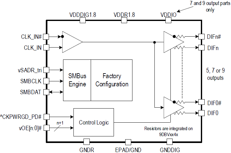
- OE# pin for each output; support DIF power management
- HCSL-compatible differential input; can be driven by common clock sources
- SMBus-selectable features allow optimization to customer requirements
- Slew rate for each output; allows tuning for various line lengths
- Differential output amplitude; allows tuning for various application environments
- 1MHz to 200MHz operating frequency
- 3.3V tolerant SMBus interface works with legacy controllers
- Selectable SMBus addresses; multiple devices can easily share an SMBus segment
- Device contains default configuration; SMBus interface is not required for device operation
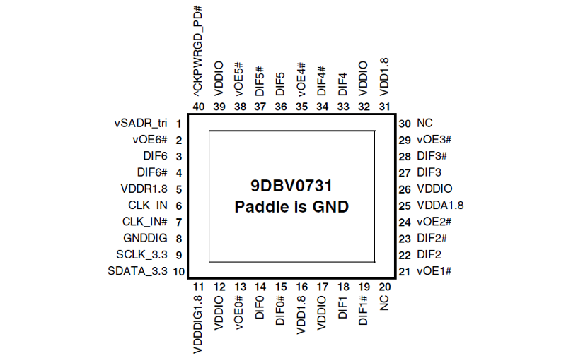
- Space-saving 5mm x 5mm 40-pin VFQFPN; minimal board space
Description
The 9DBV0731 7-output 1.8V HCSL fanout clock buffer is a member of Renesas' full-featured PCIe family. The device has seven output enables for clock management and three selectable SMBus addresses.