
特長
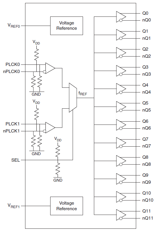
- Twelve low skew, low additive jitter LVDS output pairs
- Two selectable, differential clock input pairs
- Differential PCLK, nPCLK pairs can accept the following differential input levels: LVDS, LVPECL, CML
- Maximum input clock frequency: 2GHz (maximum)
- LVCMOS/LVTTL interface levels for the control input select pins
- Output skew: 40ps (max)
- Propagation delay: 310ps (typical)
- Low additive phase jitter, RMS; fREF = 156.25MHz,
10kHz to 20MHz: 77fs (typical) - Maximum device current consumption (IDD): 213mA
- 2.5V supply voltage
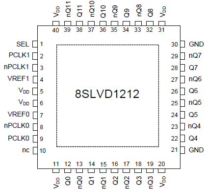
- Lead-free (RoHS 6), 40-lead VFQFN packaging
- -40 °C to 85 °C ambient operating temperature
説明
The 8SLVD1212 is a high-performance differential LVDS fanout buffer. The device is designed for the fanout of high-frequency, very low additive phase noise clock and data signals. The 8SLVD1212 is characterized to operate from a 2.5V power supply. Guaranteed output-to-output and part-to-part skew characteristics make the 8SLVD1212 ideal for those clock distribution applications demanding well-defined performance and repeatability. Two selectable differential inputs and twelve low skew outputs are available. The integrated bias voltage reference enables easy interfacing of single-ended signals to the device inputs. The device is optimized for low power consumption and low additive phase noise.
パラメータ
| 属性 | 値 |
|---|---|
| Temp. Range (°C) | -40 to 85°C |
| Product Category | Clock Buffers & Drivers, RF Buffers |
パッケージオプション
| Pkg. Type | Pkg. Dimensions (mm) | Lead Count (#) | Pitch (mm) |
|---|---|---|---|
| VFQFPN | 6.0 x 6.0 x 0.9 | 40 | 0.5 |