特長
- Fourth generation FemtoClock Next Generation (NG) technology
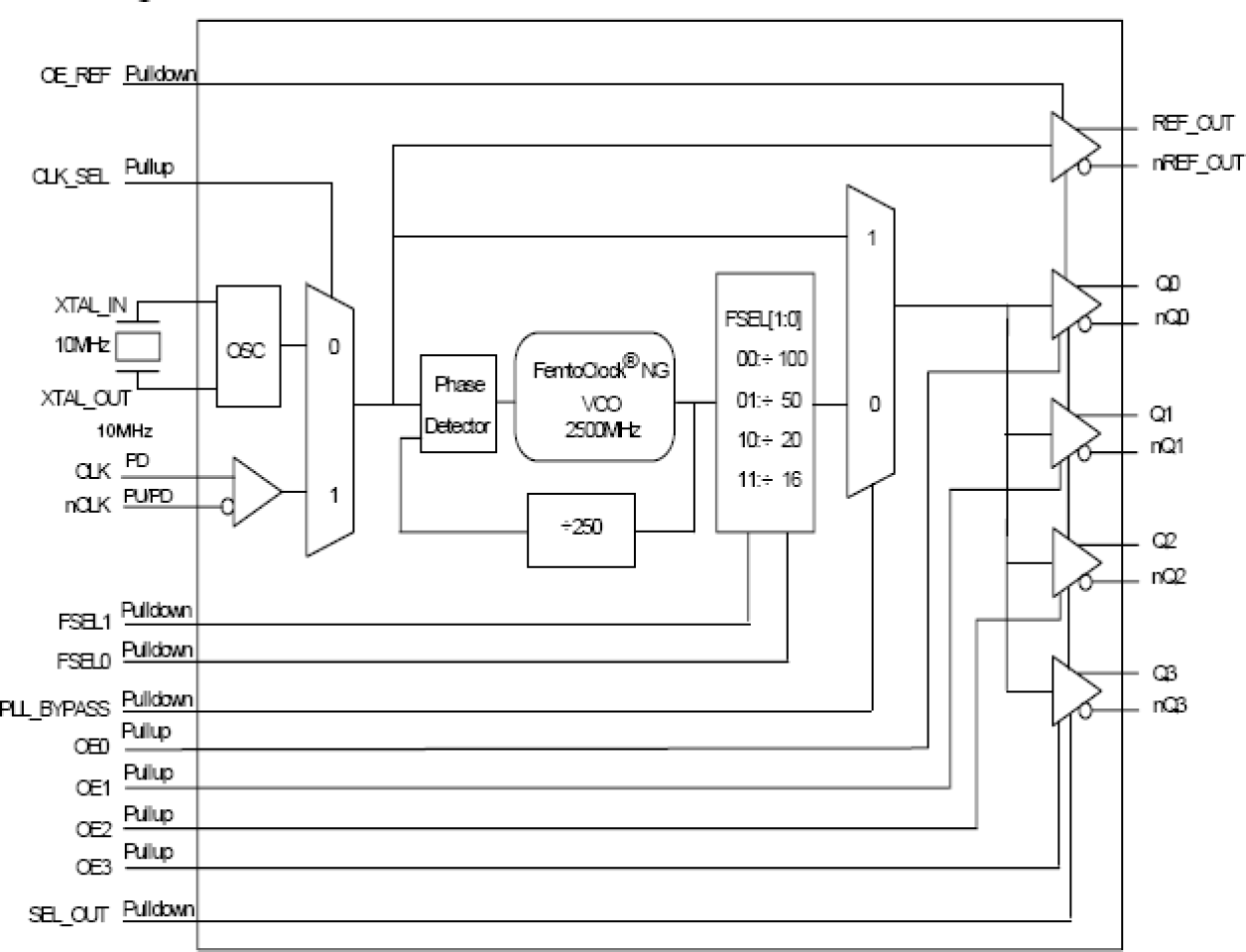
- Selectable 25MHz, 50MHz, 125MHz or 156.25MHz output clock synthesized from a 10MHz fundamental mode crystal or 10MHz differential input
- Four selectable differential LVPECL or LVDS outputs
- Crystal interface designed for 10MHz, 12pF parallel resonant crystal
- RMS phase jitter (12kHz - 20MHz): 0.336ps (typical), LVPECL outputs
- Period jitter: 2.7ps (maximum), LVPECL outputs
- Full 3.3V supply voltage
- Available in Lead-free (RoHS 6) package
- -40°C to 85°C ambient operating temperature
説明
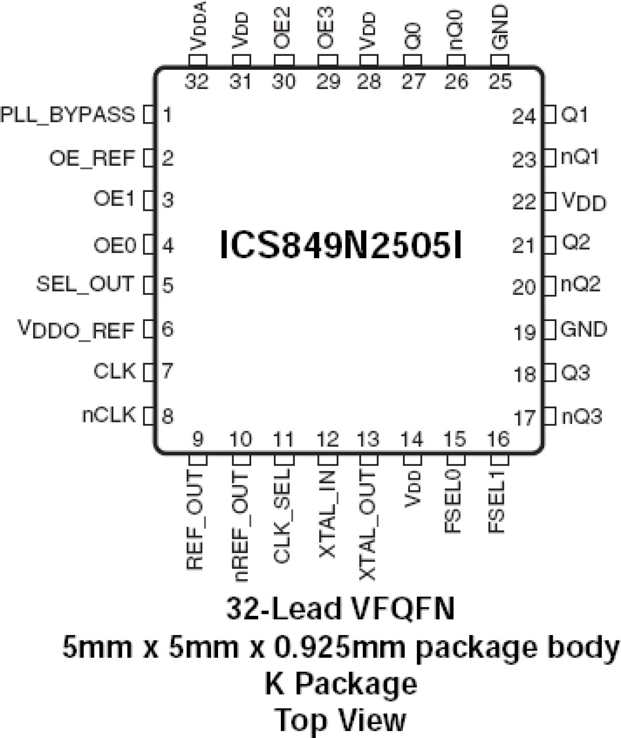
The 849N2505I is a clock synthesizer designed for wireless infrastructure applications. The device generates a selectable 25MHz, 50MHz, 125MHz or 156.25MHz clock signal from a 10MHz input with excellent phase jitter performance. The device uses IDT's fourth generation FemtoClock® NG technology for an optimum of high clock frequency and low phase noise performance, combined with a low power consumption and high power supply noise rejection. The device supports a 3.3V voltage supply and is packaged in a small, lead-free (RoHS 6) 32-lead VFQFN package. The extended temperature range supports wireless infrastructure, telecommunication and networking end equipment requirements.
適用されたフィルター


