
Package Information
| CAD Model: | View CAD Model |
| Pkg. Type: | STDFN-8 |
| Pkg. Code: | |
| Lead Count (#): | 8 |
| Pkg. Dimensions (mm): | 1.0 x 1.6 mm |
| Pitch (mm): | 0.4 |
Environmental & Export Classifications
| Moisture Sensitivity Level (MSL) | 1 |
| Pb (Lead) Free | Yes |
| ECCN (US) | |
| HTS (US) |
Product Attributes
| Lead Count (#) | 8 |
| Carrier Type | Tape & Reel |
| Moisture Sensitivity Level (MSL) | 1 |
| Pb (Lead) Free | Yes |
| Temp. Range (°C) | -40 to +85°C |
| Country of Assembly | CHINA, TAIWAN |
| Country of Wafer Fabrication | TAIWAN |
| Current Monitor Output | No |
| Discharge Circuit | Yes |
| Enable | Active High |
| FET Pass Device Type | Dual N-Channel |
| IDS (A) | 1 |
| IDS Channel 1 (A) | 1 |
| IDS Channel 2 (A) | 1 |
| Input Quiescent Current Channel 1, max (µA) | 50 |
| Input Quiescent Current Channel 1, typ (µA) | 35 |
| Input Quiescent Current when OFF Channel 1, max (µA) | 1 |
| Input Quiescent Current when OFF Channel 1, typ (µA) | 0.1 |
| Internal TVS Surge Protection | No |
| MOQ | 3000 |
| Output Discharge Circuit | Yes |
| Output Voltage Slew Rate set by | Resistor |
| Over Current Protection (OCP) | No |
| Over Temperature Protection (OTP) | Yes |
| Over Voltage Protection | No |
| Parametric Category | Load Switches |
| Pitch (mm) | 0.4 |
| Pkg. Dimensions (mm) | 1.0 x 1.6 mm |
| Pkg. Type | STDFN-8 |
| Power Good (PG), FAULT indicator | No |
| Power Monitor Output | No |
| Price (USD) | $0.39512 |
| Protection Features | TSD |
| Qty. per Reel (#) | 3000 |
| RDSON (Typ) (mΩ) | 40 |
| RDSON (Typ) Channel 1 (mΩ) | 40 |
| RDSON (Typ) Channel 2 (mΩ) | 40 |
| Ramp Control | Resistor |
| Reverse current blocking | No |
| Reverse voltage detection | No |
| Short Circuit Protection | No |
| Undervoltage Protection | No |
| VD/VIN (Max) | VDD |
| VD/VIN (Min) | 0.85 |
| VDD Range (V) (V) | 2.5 - 5.5 |
| VDD max. (V) | 5.5 |
| VDD min. (V) | 2.5 |
| VDDl-VDDh (V) | 2.5 - 5.5 |
| VIN Channel 1 max. (V) | 5.5 |
| VIN Channel 1 min. (V) | 0.85 |
| VIN Channel 2 max. (V) | 5.5 |
| VIN Channel 2 min. (V) | 0.85 |
| VIN Range (V) | 0.85 - 5.5 |
| VIN Range Channel 1 (V) | 0.85 - 5.5 |
| VIN Range Channel 2 (V) | 0.85 - 5.5 |
| VIN max. (V) | V5.5 |
| VIN min. (V) | V0.85 |
| VOUT Discharge Circuit | Yes |
Resources for SLG59M1446V
Description
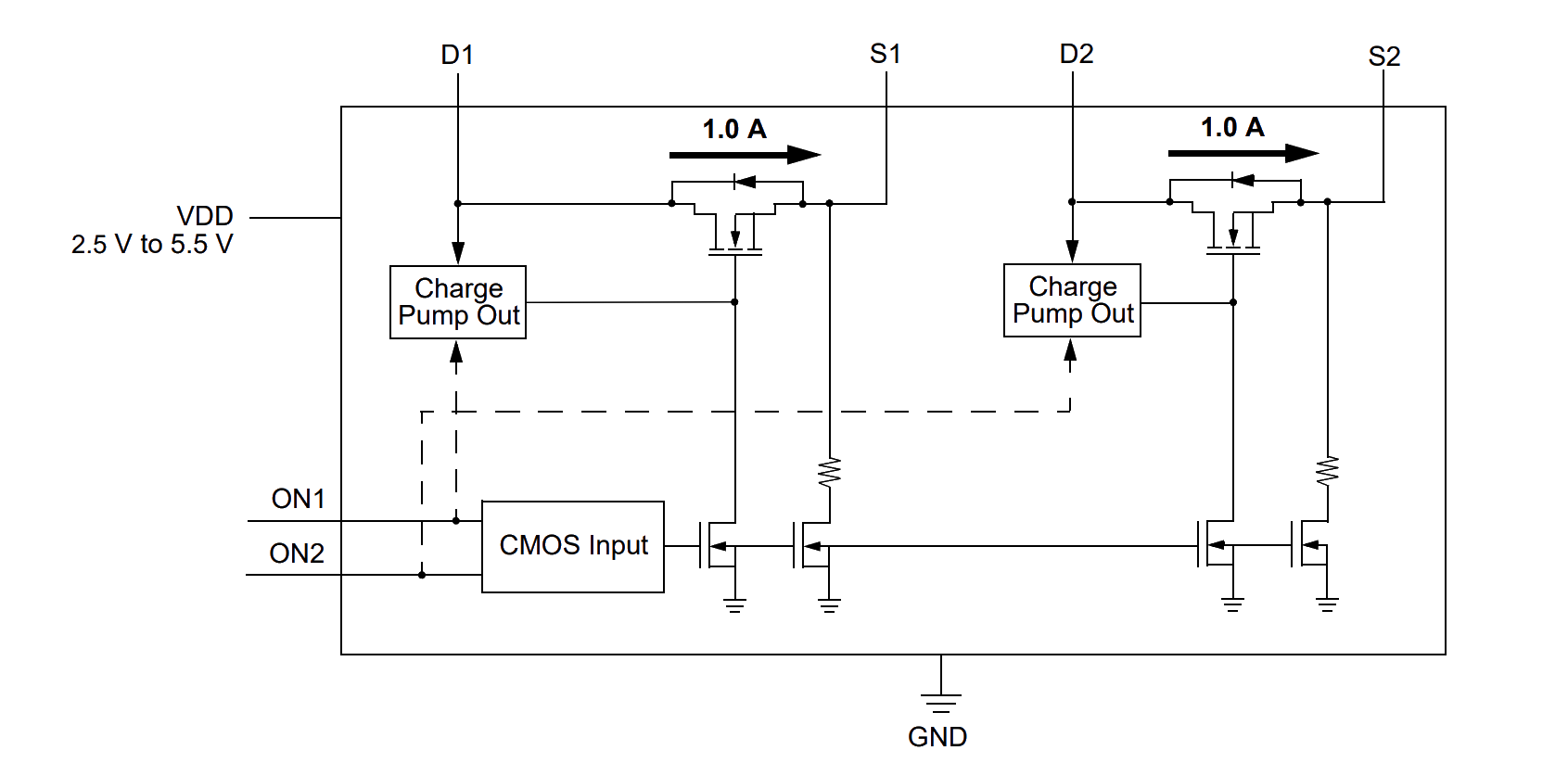
The SLG59M1446V GreenFET dual N-channel load switch is designed for load switching applications. The part comes with two 40mΩ 1.0A rated MOSFETs, each controlled by an ON control pin. The ramp rate of each MOSFET is adjustable depending on the input current level of the ON pin. The product is packaged in an ultra‑small 1.6mm x 1.0mm package.