Features
- Dense array of configurable logic
- 2240 5-bit LUTs
- 2240 D-type flip flops (DFFs)
- 10kb distributed memory
- 64kb block random access memory (BRAM)
- Power supply domains
- Two separate domains (16 GPIOs per domain)
- VDDIO0 and VDDIO1: 1.71V to 3.465V
- VDDC: 1.1V ± 5%
- Clocking
- High-frequency oscillator
- 50MHz high-frequency oscillator
- Oscillator post divider
- Divide oscillator clock by a power of 2 (range 1 to 128)
- Two independent outputs
- Phase-locked loop (PLL)
- Input from an external source, internal oscillator, or LVDS differential clock
- High-frequency oscillator
- Power-on reset (POR)
- Flexible power-consumption control
- FPGA core power control
- Clock sources power control
- BRAM deep-sleep/power-gated modes
- General-purpose IOs
- 32 GPIOs
- Flexible configuration options
- Selectable drive strength (4/8/12mA)
- Optional pull-up – 1x or 2x
- Optional pull-up control from the FPGA core
- Optional Schmitt trigger input
- Six LVDS-capable GPIOs (three true-LVDS pairs up to 100Mbps)
- Fast routing capability between pairs of GPIO located in different IO voltage domains
- Bitstream security features
- CRC integrity check
- AES decryption
- Configuration options
- OTP mode – Load from built-in OTP memory
- SPI Controller (Master) mode – Load from external Flash memory
- SPI Target (Slave) mode – Load from external source (MCU host)
- Boot control logic: Can address up to 16 different bitstreams from external memory
- Two idle low-power modes
- Sleep mode when configuration is being retained and no device re-configuration is needed
- Reset mode when device re-configuration is required after exit from this mode
- Possibility to retain GPIOs and BRAM states in both low-power modes
- Low power consumption in both modes (< 85µA)
- Operating temperature range: -40°C to 85°C
- RoHS-compliant/Halogen-free
- Available package
- SLG47920V: 40-pin QFN, 5.0mm x 5.0mm, 0.4mm pitch

Description
The SLG47920 is a small, low-power device for common FPGA applications. Users create a circuit design by programming the one-time programmable (OTP) non-volatile memory (NVM) or providing a bitstream through an SPI interface to configure the FPGA core, the IO pins, and the macrocells of the chip. This highly versatile device enables a wide range of FPGA applications.
Parameters
| Attributes | Value |
|---|---|
| Vddc | 1.05 - 1.15 |
| Vddio | 1.71 - 3.465 |
| GPIOs (#) | 32 |
| Look-up Table (LUTs) | 2240 |
| D Flip-flops (DFFs) (#) | 2240 |
| BRAM (kbit) | 64 |
| Distributed Memory (kbit) | 10 |
| Vddio Domains (#) | 2 |
| LVDS Channels (#) | 3 |
| On-chip Oscillator | Yes |
| On-chip Oscillator Freq. | 50MHz / 3MHz |
| PLLs | 2 |
| Configuration Modes | SPI Controller, SPI Target, OTP |
| Memory Type | OTP |
| Temp. Range (°C) | -40 to +85°C |
| Sleep/Reset Mode Current (µA) | 77 |
| Static State Iddc (µA) | 118 |
| Special Features | Sleep Mode,Fast Route,Bitstream AES Decryption,Boot Control |
Package Options
| Pkg. Type | Pkg. Dimensions (mm) | Lead Count (#) | Pitch (mm) |
|---|---|---|---|
| LQFN | 5.0 x 5.0 0.4 pitch | 40 | 0.4 |
Applications
- Consumer electronics
- Data communications equipment
- Handheld and portable electronics
- Notebooks and tablet PCs
- Industrial instrumentation and control
Renesas Boards & Kits
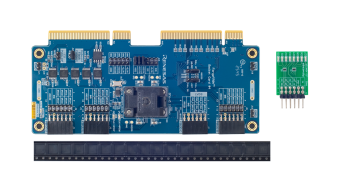
ForgeFPGA SLG47920V Socket Card Kit
The SLG47920V-SKT is a socket card kit for use with the SLG4DVKGOCONF Go Configure Development Board. The SLG47920V-SKT kit includes the ForgeFPGA™ Socket Card #4 (SLG7SC4), 20 samples of SLG47920V, and a Pmod™ LED adapter.
The ForgeFPGA™ Socket Card #4 is a development board designed for... Read More
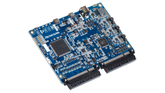
Go Configure Development Board
The Go Configure™ Development Board is a universal development board for Renesas' ForgeFPGA products that supports all features of the Go Configure™ Software Hub. A set of compatible socket cards is available for a quick and easy start to the development process. This board is ideal for rapid... Read More
Support Communities
-
SLG47910 ForgeFPGA IC Availability in 2025
The evaluation board for the SGL47910 is available, but purchasing units of the IC in less than reel qty (100..200 units) seems an impossible task, and I don't want to design something only to find out I'd be required to purchase 5000 units. When is this IC ...
Feb 6, 2025

Support Communities


