| Pkg. Type: | FCCSP |
| Pkg. Code: | AVG35 |
| Lead Count (#): | 35 |
| Pkg. Dimensions (mm): | 2.3 x 5.8 x 0.9 |
| Pitch (mm): | 0.05 |
| Moisture Sensitivity Level (MSL) | 3 |
| Pb (Lead) Free | Yes |
| ECCN (US) | EAR99 |
| HTS (US) | 8542.39.0090 |
| Pkg. Type | FCCSP |
| Lead Count (#) | 35 |
| Carrier Type | Reel |
| Moisture Sensitivity Level (MSL) | 3 |
| Qty. per Reel (#) | 4000 |
| Qty. per Carrier (#) | 0 |
| Pb (Lead) Free | Yes |
| Pb Free Category | e8 SnAgCu |
| Temp. Range (°C) | 0 to 70°C |
| Function | DDR5 Client Clock Driver |
| Input Voltage Range (V) | - |
| Length (mm) | 2.3 |
| MOQ | 4000 |
| Pitch (mm) | 0.05 |
| Pkg. Dimensions (mm) | 2.3 x 5.8 x 0.9 |
| Published | No |
| Reel Size (in) | 13 |
| Supply Voltage (V) | - |
| Tape & Reel | Yes |
| Thickness (mm) | 0.9 |
| Width (mm) | 5.8 |
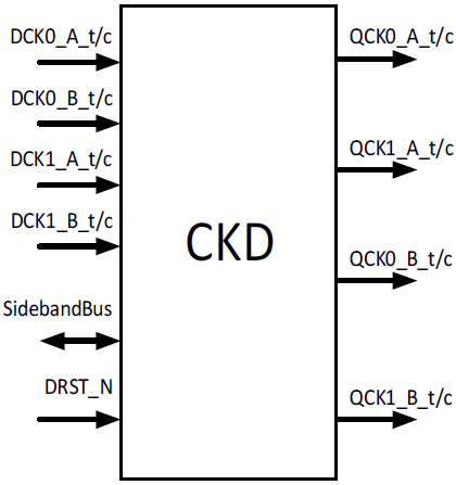
The RG5C172 Client Clock Driver (CKD) is a first-of-its-kind device designed specifically for Client DIMMs including:
The CKD buffers the clock between the host controller and DRAM, which is required for DDR5 client DIMMs operating at speeds of 6400MT/s and higher. The CKD supports speeds up to 7200MT/s.
This clock driver has I²C and I³C sideband access to enable asynchronous control and provides access to internal control words for configuring device features and adapting to different SODIMM and UDIMM configurations and memory down applications.
Renesas Clock Driver (CKD) regenerates the clock signal locally on the DIMM which ensures stable operation even at elevated clock speeds. This enhances signal integrity and reliability at high speeds, allowing DIMM data rates to operate up to 7200 MT/s.
The RG5C172 contains two separate channels with some common logic such as clocking, but otherwise operate independently of each other. Each channel has a 7-bit double data rate CA bus input, a single parity input, two chip-select inputs, produces two copies of 14-bit single data rate CA bus outputs and two copies of the chip-select outputs. The RCD has a common clock input and PLL, but produces separate clock outputs to the DRAM channels.