
| CAD Model: | View CAD Model |
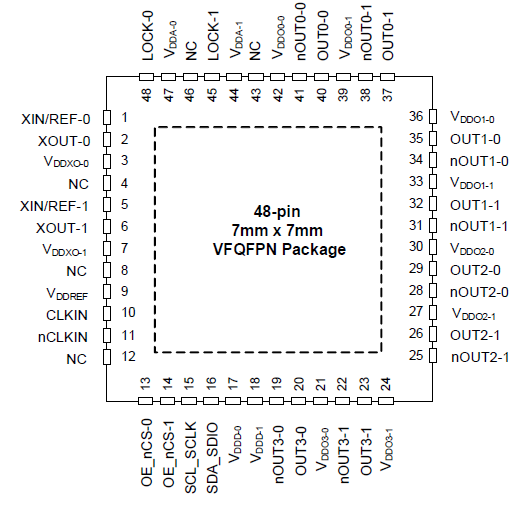
| Pkg. Type: | VFQFPN |
| Pkg. Code: | NLG48 |
| Lead Count (#): | 48 |
| Pkg. Dimensions (mm): | 7.0 x 7.0 x 0.9 |
| Pitch (mm): | 0.5 |
| Moisture Sensitivity Level (MSL) | 3 |
| Pb (Lead) Free | Yes |
| ECCN (US) | EAR99 |
| HTS (US) | 8542.39.0090 |
| Lead Count (#) | 48 |
| Carrier Type | Tray |
| Moisture Sensitivity Level (MSL) | 3 |
| Qty. per Reel (#) | 0 |
| Qty. per Carrier (#) | 260 |
| Pb (Lead) Free | Yes |
| Pb Free Category | e3 Sn |
| Temp. Range (°C) | -40 to 85°C |
| 105°C Max. Case Temp. | 0 |
| Advanced Features | SyncE, DCO, Phase Adjust, External Feedback, Hitless Switching |
| App Jitter Compliance | 112G SerDes Jitter, PCIe Gen 6 |
| Application | Switch, Router, Medical Equipment, Broadcasting Video |
| Channels (#) | 1 |
| Clock Support | T-TSC, G.8262, G.8262.1 |
| Core Voltage (V) | 1.8V, 3.3V |
| Diff. Inputs | 2 |
| Diff. Outputs | 8 |
| Family Name | FemtoClock Clock Generator |
| Fractional Output Dividers (#) | 2 |
| Input Freq (MHz) | 1 - 800 |
| Input Type | Crystal, LVPECL, HCSL, LVDS, CML, LVCMOS |
| Inputs (#) | 3 |
| Lead Compliant | No |
| Length (mm) | 7 |
| Loop Bandwidth Range (Hz) | 0.1 - 12000 |
| MOQ | 260 |
| Output Banks (#) | 8 |
| Output Freq Range (MHz) | 10 - 1000 |
| Output Skew (ps) | 40 |
| Output Type | HCSL, LVDS, LVCMOS |
| Output Voltage (V) | 1.8 |
| Outputs (#) | 8 |
| Phase Jitter Max RMS (ps) | 0.1 |
| Phase Jitter Typ RMS (fs) | 79 |
| Phase Jitter Typ RMS (ps) | 0.067 |
| Pitch (mm) | 0.5 |
| Pkg. Dimensions (mm) | 7.0 x 7.0 x 0.9 |
| Pkg. Type | VFQFPN |
| Product Category | FemtoClock 2, Ultra-Low Jitter Clocks (<300 fs RMS), Extreme Performance Clocks (<150 fs RMS), Jitter Attenuators, Network Synchronization, PDH and SONET/SDH Clocks, Programmable Clocks |
| Prog. Interface | OTP, I2C, SPI |
| Reference Output | No |
| Selection Criteria | <150 fs RM |
| Spread Spectrum | No |
| Tape & Reel | No |
| Thickness (mm) | 0.9 |
| Width (mm) | 7 |
| Xtal Freq (KHz) | 25 - 80 |
| Xtal Inputs (#) | 1 |
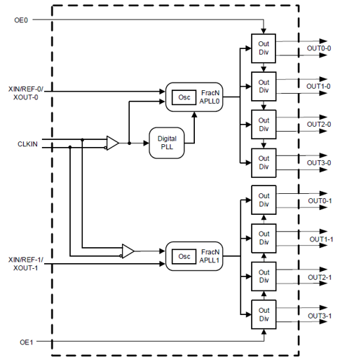
The RC32508A regenerates and distributes ultra-low jitter clock outputs and features up to two independent frequency domains that can be either locked to the external reference clock or locked to a free-run crystal or oscillator. Digital PLL (DPLL) support hitless reference switching between references from redundant timing sources. The device supports multiple independent timing channels for clock generation and jitter attenuation for high-speed serial links. Input-to-input, input-to-output, and output-to-output phase skew can all be precisely managed. The device outputs ultra-low jitter clocks that can directly synchronize SerDes running at up to 112Gbps; as well as CPRI/OBSAI, SONET/SDH ADC/DAC. The device is ideal for use in 100G/200G/400G/800G telecom switch line cards, fabric cards, and OTN applications.
