Features
- Ultra-high precision front-end amplifier
- Zero-drift instrumentation amplifier
- Pin selectable 9 gain settings: G = 1 to 1,000
- Rail-to-rail input/output
- Differential output
- RFI filtered inputs improve EMI rejection
- Single supply: 2.5V to 5.5V
- Dual supply: ±1.25V to ±2.75V
- Low input offset: 5μV, Maximum
- Low input offset drift: 50nV/°C, Maximum
- High CMRR: 138dB, G = 100
- Low gain error: <0.4%, All Gains, Maximum
- Gain bandwidth: 2.3MHz
- Input voltage noise (0.1Hz to 10Hz): 0.4μVP-P
- Operating temperature range: -40 °C to +125 °C

Description
The ISL28634 is a 5V zero-drift rail-to-rail input/output (RRIO) Programmable Gain Instrumentation Amplifiers (PGIA). This instrumentation amplifier features low offset, low noise, low gain error, and high CMRR. It is ideal for high precision applications over the wide industrial temperature range. This in-amp is designed with a unique 2-bit, 3-state logic interface that allows up to 9 selectable gain settings. The ISL2863x differential output amplifier includes a reference pin to set the common-mode output voltage to interface with differential input ADCs.
Applications
- Pressure and strain gauge transducers
- Weight scales
- Flow sensors
- Biometric: ECG/blood glucose
- Temperature sensors
- Test and measurement
- Data acquisition systems
- Low ohmic current sense
| Part Number | Status | Samples | Stock | RoHS | Package | Lead Count (#) | Carrier Type | Moisture Sensitivity Level (MSL) | Pb (Lead) Free | Pb Free Category | Temp. Range (°C) |
|---|---|---|---|---|---|---|---|---|---|---|---|
| ISL28634FVZ | Obsolete | N/A | In Stock | RoHS:EN | TSSOP | 14# | Tube | 2 | Yes | Pb-Free 100% Matte Tin Plate w/Anneal-e3 | -40 to +125°C |
| ISL28634FVZ-T13 | Obsolete | N/A | Out of Stock | RoHS:EN | TSSOP | 14# | Reel | 2 | Yes | Pb-Free 100% Matte Tin Plate w/Anneal-e3 | -40 to +125°C |
| ISL28634FVZ-T7A | Obsolete | N/A | In Stock | RoHS:EN | TSSOP | 14# | Reel | 2 | Yes | Pb-Free 100% Matte Tin Plate w/Anneal-e3 | -40 to +125°C |
Filters
Applied Filters
- Application NotePDF 992 KB R13AN0012EU0101 Rev.1.01 Feb 07, 2022AI-generated Summary: Current sensing techniques include low-side and high-side sensing using low-voltage precision op-amps combined with current sense resistors. Low-side sensing places the resistor between load and ground, offering simplicity and low cost but limited short-circuit detection. High-side sensing places the resistor between supply and load, enabling short-circuit detection but requiring higher complexity and level shifting. Current-sense resistors convert current to voltage linearly, with key parameters such as tolerance, temperature coefficient, and power rating affecting accuracy. Low-side sensing uses non-inverting amplifiers with tight offset voltage requirements, while high-side sensing employs output transistors to maintain voltage balance. Ultra-low offset amplifiers allow smaller sense resistors, reducing power loss and improving measurement range.
- Application NotePDF 284 KB r13an0006eu-bias-isl2853x-isl2863x May 15, 2020AI-generated Summary: Instrumentation amplifiers require proper DC biasing at their inputs and outputs to function correctly. Input biasing involves referencing inputs to a common-mode voltage (VCM) via bias resistors, ensuring correct transistor operation. Different sensor types, such as DC bridge sensors and thermocouples, have specific biasing needs. AC-coupled inputs require additional biasing to avoid floating inputs. Output biasing sets the output reference voltage (VREF) to center the output range, typically ground in dual supply systems or derived from the supply in single supply systems. Using a voltage reference IC for VREF improves accuracy, PSRR, and CMRR. Ratio-metric applications maintain VREF proportional to supply voltage, using buffered voltage dividers and low-pass filtering to minimize noise and errors.
- Application NotePDF 185 KB r13an0005eu-cascading-instrumentation-amplifiers May 15, 2020AI-generated Summary: Cascading instrumentation amplifiers achieves high gain while maintaining high bandwidth, overcoming the bandwidth limitations of single-stage amplifiers at high gain. Using three cascaded ISL28634 devices, each set to a gain of 10, results in an overall gain of 1000 with a bandwidth of 136kHz, significantly higher than a single amplifier at the same gain. This approach also reduces low-frequency noise compared to a single amplifier operating at high gain. Gain settings are digitally programmable and controlled via GPIO, enabling flexible gain adjustment in powers of 10 for applications requiring precise amplification with low noise and high bandwidth.
- Application NotePDF 324 KB r13an0004eu-instrumentation-amps Apr 02, 2020AI-generated Summary: High-precision instrumentation amplifiers feature zero-drift architecture, nine programmable gain settings, and rail-to-rail inputs/outputs, enabling accurate amplification of small differential signals amid large common-mode voltages. The input stage distinguishes gain for common-mode and differential signals to prevent saturation. The ISL2853x offers a single-ended output with an uncommitted zero-drift op-amp, while the ISL2863x provides a fully differential output. Gain settings are configurable via pin-strapping or microcontroller control, with internal safeguards against saturation. Practical examples include strain gauge sensor amplification and output stage operation, emphasizing precise signal conditioning across industrial temperature ranges.
- Application NotePDF 263 KB r13an0003eu0100-biasing-op-amps Dec 06, 2019AI-generated Summary: Proper biasing of operational amplifiers is essential to avoid malfunction in AC-coupled circuits. A missing DC bias path causes long stabilization times and potential failures. Adding input resistors to ground provides a DC path for bias currents, minimizing offset errors. For single-supply AC-coupled amplifiers, biasing uses a reference voltage, ideally from a high-PSRR voltage reference or buffered voltage divider, to maintain signal symmetry and reduce noise. Understanding frequency responses of input and feedback components is crucial for setting bandwidth and gain characteristics.
- Manual - Development ToolsPDF 430 KB r12uz0046eu-rkta-semitecrtdevz-user-manual Jun 11, 2019
- PCB Design FilesZIP 4.56 MB rtka-semitecrtdevzbom_design Jun 05, 2019
- Manual - Development ToolsPDF 1.21 MB r12uz0048eu-rtka-bdgstkev1z-user-manual Mar 26, 2019
- Application NotePDF 564 KB an1993 May 22, 2018AI-generated Summary: Voltage feedback (VFB) amplifiers use a differential input pair, a high-impedance stage, and an output buffer to convert input voltage differences into output voltage. The VFB amplifier's gain decreases at a dominant pole frequency due to compensation capacitors. Current feedback (CFB) amplifiers include a class AB input amplifier, current mirror, high-impedance stage, and output buffer. CFB amplifiers provide faster switching and higher slew rates by drawing charge/discharge currents directly from supply rails, unlike VFB amplifiers which are limited by biasing current sources.
- DatasheetPDF 2.21 MB isl28533-534-535-633-634-635 Aug 07, 2013
Recommended Documents (1)
- DatasheetPDF 2.21 MB isl28533-534-535-633-634-635 Aug 07, 2013
Datasheets (1)
- Manual - Development ToolsPDF 430 KB r12uz0046eu-rkta-semitecrtdevz-user-manual Jun 11, 2019
- Manual - Development ToolsPDF 1.21 MB r12uz0048eu-rtka-bdgstkev1z-user-manual Mar 26, 2019
Manuals & Guides (3)
- Application NotePDF 992 KB R13AN0012EU0101 Rev.1.01 Feb 07, 2022AI-generated Summary: Current sensing techniques include low-side and high-side sensing using low-voltage precision op-amps combined with current sense resistors. Low-side sensing places the resistor between load and ground, offering simplicity and low cost but limited short-circuit detection. High-side sensing places the resistor between supply and load, enabling short-circuit detection but requiring higher complexity and level shifting. Current-sense resistors convert current to voltage linearly, with key parameters such as tolerance, temperature coefficient, and power rating affecting accuracy. Low-side sensing uses non-inverting amplifiers with tight offset voltage requirements, while high-side sensing employs output transistors to maintain voltage balance. Ultra-low offset amplifiers allow smaller sense resistors, reducing power loss and improving measurement range.
- Application NotePDF 284 KB r13an0006eu-bias-isl2853x-isl2863x May 15, 2020AI-generated Summary: Instrumentation amplifiers require proper DC biasing at their inputs and outputs to function correctly. Input biasing involves referencing inputs to a common-mode voltage (VCM) via bias resistors, ensuring correct transistor operation. Different sensor types, such as DC bridge sensors and thermocouples, have specific biasing needs. AC-coupled inputs require additional biasing to avoid floating inputs. Output biasing sets the output reference voltage (VREF) to center the output range, typically ground in dual supply systems or derived from the supply in single supply systems. Using a voltage reference IC for VREF improves accuracy, PSRR, and CMRR. Ratio-metric applications maintain VREF proportional to supply voltage, using buffered voltage dividers and low-pass filtering to minimize noise and errors.
- Application NotePDF 185 KB r13an0005eu-cascading-instrumentation-amplifiers May 15, 2020AI-generated Summary: Cascading instrumentation amplifiers achieves high gain while maintaining high bandwidth, overcoming the bandwidth limitations of single-stage amplifiers at high gain. Using three cascaded ISL28634 devices, each set to a gain of 10, results in an overall gain of 1000 with a bandwidth of 136kHz, significantly higher than a single amplifier at the same gain. This approach also reduces low-frequency noise compared to a single amplifier operating at high gain. Gain settings are digitally programmable and controlled via GPIO, enabling flexible gain adjustment in powers of 10 for applications requiring precise amplification with low noise and high bandwidth.
- Application NotePDF 324 KB r13an0004eu-instrumentation-amps Apr 02, 2020AI-generated Summary: High-precision instrumentation amplifiers feature zero-drift architecture, nine programmable gain settings, and rail-to-rail inputs/outputs, enabling accurate amplification of small differential signals amid large common-mode voltages. The input stage distinguishes gain for common-mode and differential signals to prevent saturation. The ISL2853x offers a single-ended output with an uncommitted zero-drift op-amp, while the ISL2863x provides a fully differential output. Gain settings are configurable via pin-strapping or microcontroller control, with internal safeguards against saturation. Practical examples include strain gauge sensor amplification and output stage operation, emphasizing precise signal conditioning across industrial temperature ranges.
- Application NotePDF 263 KB r13an0003eu0100-biasing-op-amps Dec 06, 2019AI-generated Summary: Proper biasing of operational amplifiers is essential to avoid malfunction in AC-coupled circuits. A missing DC bias path causes long stabilization times and potential failures. Adding input resistors to ground provides a DC path for bias currents, minimizing offset errors. For single-supply AC-coupled amplifiers, biasing uses a reference voltage, ideally from a high-PSRR voltage reference or buffered voltage divider, to maintain signal symmetry and reduce noise. Understanding frequency responses of input and feedback components is crucial for setting bandwidth and gain characteristics.View More (8)
Application Notes & White Papers (8)
Product Notices (PCN, EOL, etc) (2)
No Results Found.
Make sure all keywords are spelled correctly.
Try fewer, different, or more general terms to vary your search.
If you have filters applied, consider deselecting some to broaden your results.
- Search our extensive knowledgebase, designed to help customers with their FAQs.
- Get help from our expert Renesas technical staff and community on our support forums.
- PCB Design FilesZIP 4.56 MB rtka-semitecrtdevzbom_design Jun 05, 2019
Schematics & Design Files (3)
No Results Found.
Make sure all keywords are spelled correctly.
Try fewer, different, or more general terms to vary your search.
If you have filters applied, consider deselecting some to broaden your results.
- Search our extensive knowledgebase, designed to help customers with their FAQs.
- Get help from our expert Renesas technical staff and community on our support forums.
Marketing Collateral (1)
Other (1)
No Results Found.
Make sure all keywords are spelled correctly.
Try fewer, different, or more general terms to vary your search.
If you have filters applied, consider deselecting some to broaden your results.
- Search our extensive knowledgebase, designed to help customers with their FAQs.
- Get help from our expert Renesas technical staff and community on our support forums.
Renesas Boards & Kits
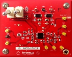
5V, Rail-Rail I/O, Zero-Drift, Differential Output, Programmable Gain Instrumentation Amplifier Evaluation Board
The ISL28634EV2Z board allows simple evaluation of the ISL28634 5V zero-drift programmable gain instrumentation amplifier. The board is designed with all the necessary components to easily connect the high-performance amplifier to an external signal. It can operate from a single supply of +2.5V... Read More
