Overview
Description
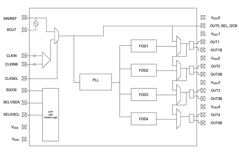
The 5P49V5901 is a low-power programmable clock generator with best-in-class jitter performance and design flexibility with universal outputs capable of generating any output frequency. The 5P49V5901 is intended for high-performance consumer, networking, industrial, computing, and data communications applications. Configurations may be stored in on-chip One-Time Programmable (OTP) memory or changed using the I2C interface. This is Renesas' fifth generation of programmable clock technology (VersaClock® 5). The frequencies are generated from a single reference clock or crystal input. A glitchless manual switchover function allows one of the redundant clock inputs to be selected during normal operation.
Two select pins allow up to four different configurations to be programmed and accessible using processor GPIOs or bootstrapping. The different selections may be used for different operating modes (full function, partial function, and partial power-down), regional standards (US, Japan, Europe), or system production margin testing. The device may be configured to use one of two I2C addresses to allow multiple devices to be used in a system.
Features
- 4 differential outputs LVPECL, LVDS, HCSL - or 8 LVCMOS outputs
- In-system programmable with 4 independent output frequencies
- Up to 350MHz input/output frequencies
- Also supports crystal input
- Stores 4 different configurations in OTP non-volatile memory
- < 100mW core power (at 3.3V)
- < 0.7ps RMS phase jitter (typ.)
- Meets PCIe® Gen 1/2/3, USB 3.0, 1/10 GbE clock requirements
- 1.8V/2.5V/V3.3V core and output voltages
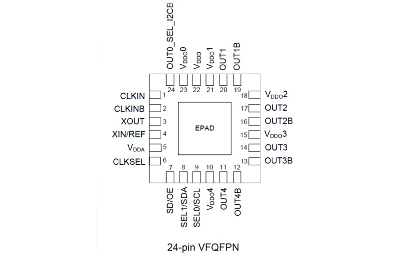
- 4mm x 4mm 24-lead VFQFPN
- -40 °C to +85 °C operating temperature range
- Supported by the Timing Commander™ software tool
Comparison
Applications
Design & Development
Software & Tools
Boards & Kits
Models
ECAD Models
Schematic symbols, PCB footprints, and 3D CAD models from SamacSys can be found by clicking on the CAD Model links in the Product Options table. If a symbol or model isn't available, it can be requested directly from SamacSys.

Support

Support Communities


Support Communities
-
Reliability >> Failure Rate >> (FIT/MTTF/MTBF) 5P49V5901
Hi, Where could I locate a failure rate (FIT or MTTF or MTFB) for the 5P49V5901 (VersaClock 5 Low Power Programmable Clock Generator)? Thank you, CJR
Jul 24, 2023 -
Versa 5 phase noise
We are programming the clock the first time. Phase noise tested is 10dB worse than the phase noise shown in datasheet for region from 1MHz offset and above (outside the PLL loop). What could be wrong? Also notice your plot has 15dBm output. Did you use external amplifier? Thanks, [locked ...
Jul 13, 2022 -
5P49V60 OUT0 dropout and OTP Programming
In my design, I'm using a 19.2MHz crystal and outputting a variety of clocks at 1.8V. I don't have a lot of choice of the 19.2MHz--it's required by the CPU I'm clocking on OUT0. A 19.2MHz crystal requires reprogramming the feedback ...
Nov 19, 2023
FAQs
-
How many device configurations can be stored in VersaClock 5 Programmable Clock Generator - 5P49V5901A?
VersaClock 5 5P49V5901A has 4 banks of One Time Programmable Memory which allows 4 devices configurations to be stored in the device. The device configurations can be selected using the Sel1, Sel0 pins. For other questions not addressed by the Knowledge Base, please submit a technical support request.
Oct 31, 2016 -
What is the core power (current) consumption of VersaClock 5 Programmable Clock Generator - 5P49V5901A?
30 mA (typ). For other questions not addressed by the Knowledge Base, please submit a technical support request.
Oct 31, 2016 -
How to calculate the PLL Fractional Feedback Divider for IDTs 5P49V5901 VersaClock 5 Programmable Clock Generator device
The PLL feedback divider M is composed of a 12 bit integer portion, FB_intdiv[11:0] and a 24 bit fractional portion, FB_frcdiv[23:0]. Convert FRAC(M) to hex with Eq.2 where ROUND2INT means to round to the nearest integer. The round-off error of M ...
Oct 31, 2016