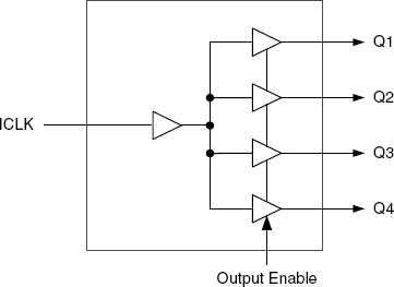
Features
- Low skew (250 ps) outputs
- Pb-free packaging
- Low cost clock buffer
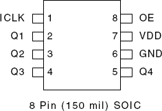
- Packaged in 8-pin SOIC
- Input/Output clock frequency up to 160 MHz
- Non-inverting output clock
- Ideal for networking clocks
- Operating Voltages of 3.3 and 5.0 V
- Output Enable mode tri-states outputs
- Advanced, low power CMOS process
- Commercial and industrial temperature versions
Description
The 551 is a low cost, high-speed single input to four output clock buffer. Part of Renesas' ClockBlocksTM family, this is our lowest cost, small clock buffer. See the 552-02B for monolithic dual version of the 551 in a 20 pin QSOP. IDT makes many non-PLL and PLL based low skew output devices as well as Zero Delay Buffers to synchronize clocks. Contact Renesas for all of your clocking needs.
Parameters
| Attributes | Value |
|---|---|
| Function | Buffer |
| Outputs (#) | 4 |
| Output Type | LVCMOS |
| Output Freq Range (MHz) | 0 - 160 |
| Input Type | LVCMOS |
| Output Banks (#) | 1 |
| Output Voltage (V) | 3.3, 5 |
| Output Skew (ps) | 250 |
Package Options
| Pkg. Type | Pkg. Dimensions (mm) | Lead Count (#) | Pitch (mm) |
|---|---|---|---|
| SOIC | 4.9 x 3.9 x 1.5 | 8 | 1.27 |