
| CAD Model: | View CAD Model |
| Pkg. Type: | VFQFPN |
| Pkg. Code: | NBG24 |
| Lead Count (#): | 24 |
| Pkg. Dimensions (mm): | 4.0 x 4.0 x 0.8 |
| Pitch (mm): | 0.5 |
| Moisture Sensitivity Level (MSL) | 1 |
| Pb (Lead) Free | Yes |
| ECCN (US) | EAR99 |
| HTS (US) | 8542.39.0090 |
| Lead Count (#) | 24 |
| Carrier Type | Tray |
| Moisture Sensitivity Level (MSL) | 1 |
| Phase Jitter Typ RMS (ps) | 0.261 |
| Input Freq (MHz) | 25 - 25 |
| Supply Voltage (V) | 1.8 - 1.8, 2.5 - 2.5, 3.3 - 3.3 |
| Xtal Freq (MHz) | 25 - 25 |
| App Jitter Compliance | PCIe Gen1, PCIe Gen2, PCIe Gen3, PCIe Gen4 |
| Core Voltage (V) | 3.3V |
| Diff. Output Signaling | LVDS |
| Output Freq Range (MHz) | 50 - 50, 100 - 100, 125 - 125, 156.25 - 156.25 |
| Output Type | LVDS |
| Output Voltage (V) | 3.3V |
| Pkg. Dimensions (mm) | 4.0 x 4.0 x 0.8 |
| Power Consumption Typ (mW) | 200 |
| Prog. Clock | No |
| Qty. per Reel (#) | 0 |
| Qty. per Carrier (#) | 490 |
| Pb (Lead) Free | Yes |
| Pb Free Category | e3 Sn |
| Temp. Range (°C) | -40 to 85°C |
| Accepts Spread Spec Input | No |
| Advanced Features | Programmable Clock |
| Architecture | Common, SRNS |
| C-C Jitter Max P-P (ps) | 50 |
| Diff. Outputs | 4 |
| Family Name | PhiClock |
| Function | Generator |
| Input Type | Crystal, LVCMOS |
| Inputs (#) | 1 |
| Length (mm) | 4 |
| MOQ | 490 |
| Output Banks (#) | 1 |
| Output Impedance | 100 |
| Outputs (#) | 4 |
| Package Area (mm²) | 25 |
| Pitch (mm) | 0.5 |
| Pkg. Type | VFQFPN |
| Product Category | PhiClock, PCI Express Clocks, Programmable Clocks |
| Reference Output | No |
| Spread Spectrum | No |
| Tape & Reel | No |
| Thickness (mm) | 0.8 |
| Width (mm) | 4 |
| Xtal Inputs (#) | 1 |
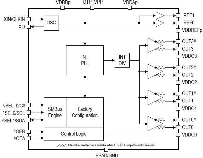
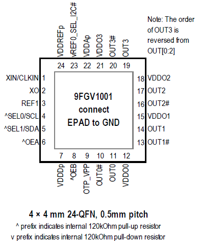
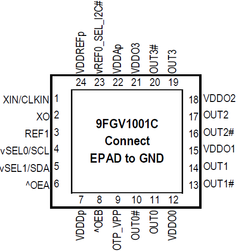
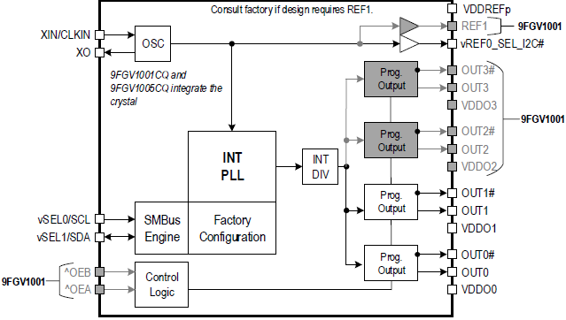
The 9FGV1001 is a member of Renesas' PhiClock™ programmable clock generator family. The 9FGV1001 provides four non-spread-spectrum copies of a single output frequency and two copies of the crystal reference input. Two select pins allow for hardware selection of the desired configuration, or two I²C bits allow easy software selection of the desired configuration. The user may configure any one of the four OTP configurations as the default when operating in I²C mode. Four unique I²C addresses are available, allowing easy I²C access to multiple components.
