

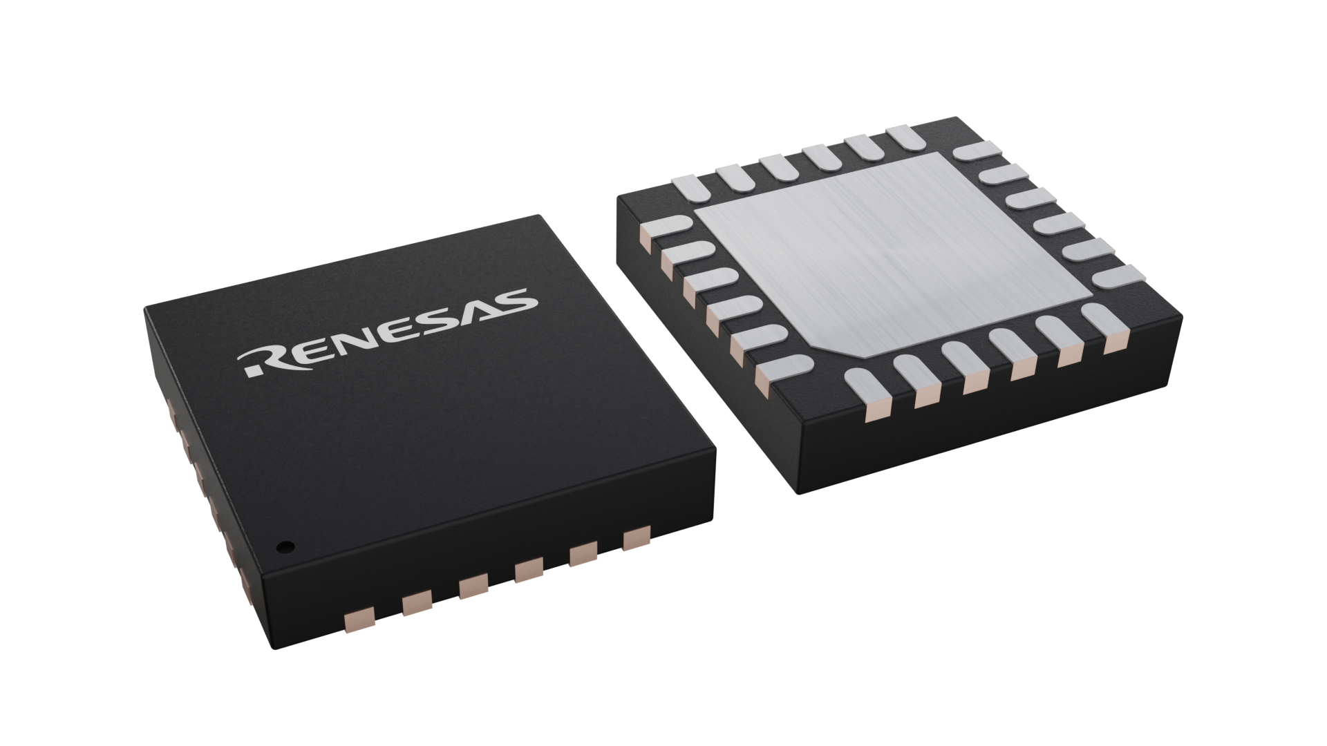

| CAD Model: | View CAD Model |
| Pkg. Type: | VFQFPN |
| Pkg. Code: | NLG24 |
| Lead Count (#): | 24 |
| Pkg. Dimensions (mm): | 4.0 x 4.0 x 0.9 |
| Pitch (mm): | 0.5 |
| Moisture Sensitivity Level (MSL) | 1 |
| Pb (Lead) Free | Yes |
| ECCN (US) | EAR99 |
| HTS (US) | 8542.39.0090 |
| Lead Count (#) | 24 |
| Carrier Type | Tray |
| Moisture Sensitivity Level (MSL) | 1 |
| Output Impedance | 100 |
| Qty. per Reel (#) | 0 |
| Qty. per Carrier (#) | 490 |
| Pb (Lead) Free | Yes |
| Pb Free Category | e3 Sn |
| Temp. Range (°C) | -40 to 85°C |
| Assembly Location | MALAYSIA |
| Wafer Fab Location | TAIWAN |
| Accepts Spread Spec Input | Yes |
| Additive Phase Jitter Typ RMS (fs) | 350 |
| Additive Phase Jitter Typ RMS (ps) | 0.35 |
| Advanced Features | Asynch or Glitch-Free Switching Mode |
| App Jitter Compliance | PCIe Gen1, PCIe Gen2, PCIe Gen3, PCIe Gen4, PCIe Gen5 |
| Architecture | Common, SRNS, SRIS |
| C-C Jitter Max P-P (ps) | 50 |
| Core Voltage (V) | 3.3V |
| Diff. Input Signaling | HCSL |
| Diff. Inputs | 2 |
| Diff. Output Signaling | LP-HCSL |
| Diff. Outputs | 4 |
| Function | Multiplexer |
| Input Freq (MHz) | 1 - 200 |
| Input Type | HCSL |
| Inputs (#) | 2 |
| Length (mm) | 4 |
| MOQ | 490 |
| Output Banks (#) | 1 |
| Output Freq Range (MHz) | 1 - 200 |
| Output Skew (ps) | 50 |
| Output Type | LP-HCSL |
| Output Voltage (V) | 0.8V |
| Outputs (#) | 4 |
| Pitch (mm) | 0.5 |
| Pkg. Dimensions (mm) | 4.0 x 4.0 x 0.9 |
| Pkg. Type | VFQFPN |
| Power Consumption Typ (mW) | 76 |
| Product Category | Clock Multiplexers, PCI Express Clocks |
| Prog. Clock | No |
| Supply Voltage (V) | 3.3 - 3.3 |
| Tape & Reel | No |
| Thickness (mm) | 0.9 |
| Width (mm) | 4 |
The 9DML04 devices are 3.3V members of Renesas' full-featured PCIe family. The 9DML04 supports PCIe Gen 1–7 Common Clocked (CC), Separate Reference no Spread (SRnS), and Separate Reference Independent Spread (SRIS) architectures. The part provides a choice of asynchronous and glitch-free switching modes and offers a choice of integrated output terminations providing direct connection to 85Ω or 100Ω transmission lines. The 9DML04P1 can be factory programmed with a user-defined power-up default SMBus configuration.
For information regarding evaluation boards and material, please contact your local sales representative.