
| CAD Model: | View CAD Model |
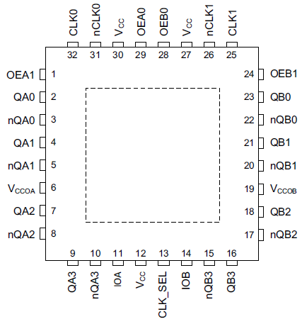
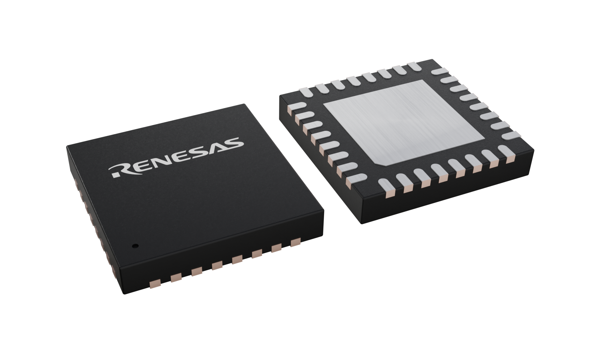
| Pkg. Type: | VFQFPN |
| Pkg. Code: | NLG32 |
| Lead Count (#): | 32 |
| Pkg. Dimensions (mm): | 5.0 x 5.0 x 0.9 |
| Pitch (mm): | 0.5 |
| Moisture Sensitivity Level (MSL) | 3 |
| Pb (Lead) Free | Yes |
| ECCN (US) | EAR99 |
| HTS (US) | 8542.39.0090 |
| Lead Count (#) | 32 |
| Carrier Type | Tray |
| Moisture Sensitivity Level (MSL) | 3 |
| Output Type | LVPECL, LVCMOS, LVDS |
| Qty. per Reel (#) | 0 |
| Qty. per Carrier (#) | 490 |
| Pb (Lead) Free | Yes |
| Pb Free Category | e3 Sn |
| Temp. Range (°C) | -40 to 85°C |
| Country of Assembly | THAILAND |
| Country of Wafer Fabrication | SINGAPORE |
| Additive Phase Jitter Typ RMS (fs) | 80 |
| Additive Phase Jitter Typ RMS (ps) | 0.08 |
| Adjustable Phase | No |
| Channels (#) | 2 |
| Core Voltage (V) | 1.8V, 2.5V, 3.3V |
| Family Name | 8P79 |
| Function | Buffer, Multiplexer, Divider |
| Input Type | LVDS, LVPECL, LVHSTL, CSL, LVCMOS |
| Inputs (#) | 2 |
| Length (mm) | 5 |
| MOQ | 490 |
| Noise Floor (dBc/Hz) | -156 |
| Output Banks (#) | 2 |
| Output Skew (ps) | 100 |
| Output Voltage (V) | 1.8V, 2.5V, 3.3V |
| Outputs (#) | 8 |
| Pitch (mm) | 0.5 |
| Pkg. Dimensions (mm) | 5.0 x 5.0 x 0.9 |
| Pkg. Type | VFQFPN |
| Price (USD) | $7.62601 |
| Product Category | Clock Buffers & Drivers, RF Buffers |
| Prog. Interface | Pin select |
| Requires Terms and Conditions | Does not require acceptance of Terms and Conditions |
| Tape & Reel | No |
| Thickness (mm) | 0.9 |
| Width (mm) | 5 |
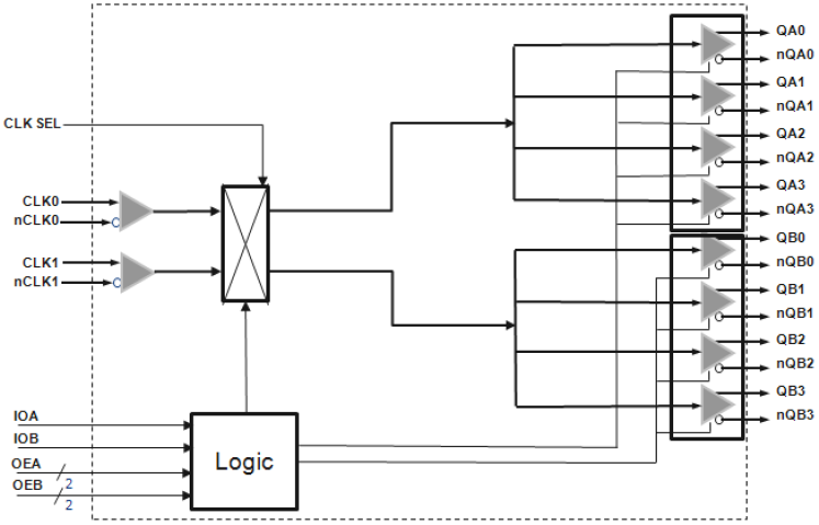
The 8P791208 is a low additive jitter 2:8 buffer with CMOS / differential outputs. The device takes 1 or 2 reference clocks, selects between them, using a pin selection and generates up to 8 outputs that are the same as the reference frequency. The 8P791208 supports two output banks, each with its own power supply. All outputs in one bank generate the same output frequency, but each output can be individually controlled for output type or output enable. The device can operate over the -40°C to 85°C temperature range.
