
Features
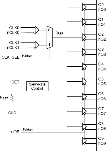
- Two differential input reference clocks
- Differential pair can accept the following differential input levels: LVPECL, LVDS
- Ten LVDS outputs
- Maximum clock frequency: 200MHz
- Output slew rate control
- Fail-safe differential inputs
- LVCMOS interface levels for all control inputs
- Output skew: 260ps (maximum), for fastest slew rate setting of 0.650 V/ns
- Part-to-part skew: 1.2ns (maximum)
- Full 2.5V supply voltage
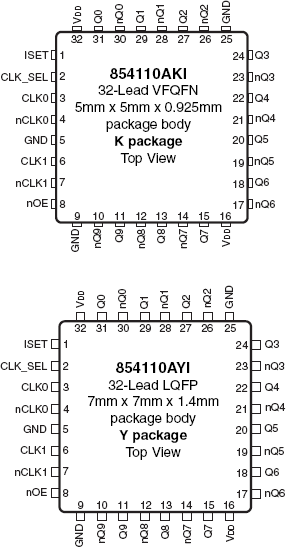
- Lead-free (RoHS 6) 32-Lead VFQFN and 32-Lead LQFP package
- -40°C to 85°C ambient operating temperature
Description
The 854110I is a high-performance differential LVDS clock fanout buffer. The device is designed for signal fanout of high-frequency, low phase-noise clock signals. The selected differential input signal is distributed to ten differential LVDS outputs. The 854110I is characterized to operate from a 2.5V power supply. Guaranteed output-to-output and part-to-part skew characteristics make the 854110I ideal for those clock distribution applications demanding well-defined performance and repeatability. The device offers an output slew rate control with four pre-set output transition times to solve crosstalk and EMI problems in complex board designs. A fail-safe input design forces the outputs to a defined state if differential clock inputs are open or shorted, see Table 3D.

Support Communities


