
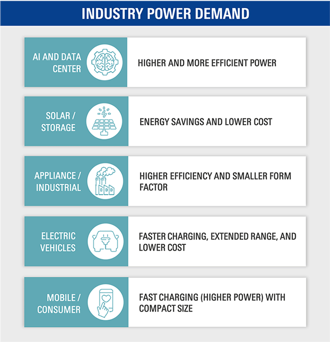
Conventional silicon semiconductors are struggling to meet the performance, density, and efficiency benchmarks required to effectively power next-generation computing and energy conversion platforms ranging from AI-optimized data centers to electric vehicles and industrial robotics. This is becoming increasingly apparent amid a shift to higher-frequency applications that demand faster switching speeds, operate with the lowest losses, and have less room to accommodate bulky heat sinks and cooling systems.
Wide bandgap semiconductors, specifically gallium nitride (GaN), are stepping into the breach to overcome the physical limitations of silicon and silicon-carbide (SiC) materials, with an inherently superior figure of merit. Thanks to faster switching frequencies, lower conduction and switching losses, and better thermal management, GaN yields compact power supplies that support AI and high-performance computing (HPC) workloads in power-dense data center racks. GaN reduces weight and helps extend driving range in EV onboard chargers and DC/DC converters. And GaN enables more efficient motor drives in factory-floor robotics as well as efficient and compact renewable energy systems like uninterruptible power supplies and PV microinverters.
Renesas and Our GaN Journey
Anticipating our customers' needs, Renesas has steadily expanded our GaN portfolio, most notably through the 2024 acquisition of Transphorm, a GaN pioneer with technological roots in the University of California, Santa Barbara, and its renowned Solid State Lighting and Energy Electronics Center (SSLEEC).
Backed by 17 years of IP and GaN products maturation, Transphorm's SuperGaN® technology platform is based on a normally off depletion-mode (d-mode) GaN-based FET, combining a high-voltage d-mode GaN HEMT device with a low-voltage silicon MOSFET. This combines the high voltage switching performance benefits of GaN with the ease of use and robustness of a silicon-based drive input interface to simplify adoption across a spectrum of high-performance and high-reliability applications.
The acquisition, which included more than 1,000 directly owned and licensed patents, gave Renesas control of Transphorm's GaN intellectual property, products, and manufacturing, including production capacity in Japan and Taiwan and R&D in California. Earlier this year, Renesas announced an agreement with Polar Semiconductor in Minnesota to manufacture 200mm GaN-on-silicon devices starting in 2027, expanding access to a key U.S. manufacturing source.
By combining GaN with Renesas' power controllers and drivers (including integrated IC+GaN products) and a broad portfolio of microcontrollers with Winning Combination reference designs, we will deliver turnkey GaN-based solutions that address everything from fast chargers to megawatt-class AI servers in the coming years.

Where GaN Is Having the Biggest Impact
When it comes to GaN adoption, data centers are the most visible beneficiary today. To accommodate AI and HPC workloads, server racks that once consumed tens of kilowatts are now scaling up to 600kW per rack, with AC/DC conversion systems reaching 1MW. In addition to power density, AI-enhanced data centers benefit from bidirectional power conversion topologies like the Vienna converter and higher switching frequencies to manage a growing footprint. Hyperscale data centers have ballooned from about 10,000 square feet 10 years ago to more than a million square feet today, even as operators look to triple the capacity inside each data center by the end of the decade¹
GaN's low switching losses, efficiency, and ability to operate at higher frequencies than both Si and SiC, enable advanced topologies such as high-density DC/DC converters and bridgeless totem-pole power factor correction with 99 percent efficiency. In July, Renesas launched three new 650V Gen IV Plus GaN FETs, the first major product release since the Transphorm acquisition, all built on a die 14 percent smaller than the previous generation and with a 20 percent better figure of merit.
GaN Sets Its Sights on EVs and Industrial Robots
GaN is also well-suited for onboard electric vehicle chargers and DC/DC converters. With a unique bidirectional device (BDS) enabled by GaN's lateral architecture, GaN simplifies AC/DC conversion topologies requiring bidirectional power flow, cuts parts count, and improves system efficiency while reducing charging subsystem size and weight. GaN technology has already been introduced to Tier 1 suppliers and automakers, and its adoption is expected to begin as early as the 2030 model year and beyond.
While SiC currently dominates traction inverters, GaN is expected to first make inroads in charging and auxiliary systems where power density is critical and eventually into traction, which aggressive EV ODMs/OEMs are already investigating. In industrial robotics and automation products, efficiency, reliability, and compact form factors are paramount. GaN enables high-efficiency servo and AC drives with smaller form factors by impacting the efficiency of the drive and motor system together. This translates to lighter, more agile robotic arms and lower system costs.
GaN Challenges and Opportunities
The potential of GaN is made clear with each successive product generation, with the migration from 150mm to 200mm wafers underway and a longer-term roadmap indicating a shift to 300mm wafers to match silicon economics. Renesas' differentiation lies in our proven d-mode high-voltage SuperGaN technology, our ability to integrate GaN with controllers and drivers and our world-class system-level design support.
To ensure we meet the rigorous specifications required by high-reliability markets such as automotive and industrial automation, Renesas' GaN portfolio exceeds today's JEDEC JESD47 standard for semiconductor qualification and achieves high reliability under switching conditions like HTOL life tests. In addition, our latest Gen4 plus platform will be ready to meet automotive qualification (AEC Q101) by mid-2027. Advanced packaging is another key consideration for reducing GaN parasitics and optimizing thermal performance. Renesas GaN is available in one of the widest packaging portfolios in the industry, including emerging top-side cooled packages (TOLT) and integrated driver-FET solutions.
Each of these design and manufacturing challenges is also an opportunity to scale more efficiently, set reliability benchmarks, standardize packaging, and help customers move from discrete devices to system-level solutions.
Looking Ahead: The Future of GaN at Renesas
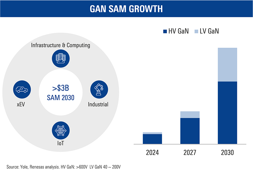
The megatrends driving GaN into the heart of AI data centers, the drivetrains of electric vehicles, the servos of industrial robots, and renewable energy power conversion systems are accelerating. In addition to our well-established high-voltage GaN (650V+), we are developing low-voltage GaN (40V - 200V) products to extend benefits to secondary-side power conversion in areas like AI high-voltage direct current (HVDC) systems (48V down to 12V or 1V), PC client computing, and battery management, industrial power tools, and e-mobility. This strategy positions GaN to become the centerpiece of our wide bandgap portfolio and will shape the next decade of power electronics by leveraging our extensive system expertise across microcontrollers, SoCs, analog, and power management. Wherever density, efficiency, and reliability are required, GaN can deliver.
Renesas, through its acquisition of Transphorm and continued investment in GaN innovation, is building the scale, reputation, and ecosystem support to make GaN a mainstream technology. The challenges of manufacturing, packaging, and qualification of new products and larger diameter wafers are significant, but so are the opportunities to redefine power electronics.
Looking ahead, Renesas' expanding GaN portfolio promises to empower designers with smaller, faster, more efficient, and more reliable systems that will enable the next generation of power electronics to build a safer, smarter, and more sustainable future.
References
1O. Johnson, CRN, "AWS, Meta, Microsoft, Nvidia, And Oracle: Five Data Center Deals Worth $676B Announced This Month" (Jan. 2025)
News & Additional Resources
| Title | Type | Date |
|---|---|---|
| Renesas Strengthens Power Leadership with New GaN FETs for High-Density Power Conversion in AI Data Centers, Industrial and Charging Systems | News | Jul 1, 2025 |
| Renesas Completes Acquisition of Transphorm | News | Jun 20, 2024 |
| Renesas to Acquire Transphorm to Expand its Power Portfolio with GaN Technology | News | Jan 11, 2024 |