特長
- Six differential LVPECL output pairs
- One differential clock input
- CLK and nCLK supports the following input types: LVPECL, LVDS, LVHSTL, SSTL, HCSL
- Maximum output frequency: 140MHz
- Input frequency range: 90MHz - 140MHz
- VCO range: 450MHz - 700MHz
- Output skew: 135ps (maximum)
- Cycle-to-Cycle jitter: 30ps (maximum)
- RMS phase jitter @ 100MHz, (1.5MHz - 22MHz): 3ps (typical)
- 3.3V operating supply
- 0°C to 70°C ambient operating temperature
- Available in lead-free (RoHS 6) package
- Industrial temperature information available upon request
説明
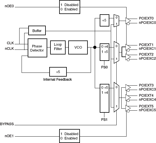
The 9DB306 is a high performance 1-to-6 Differential-to- LVPECL Jitter Attenuator designed for use in PCI Express systems. In some PCI Express systems, such as those found in desktop PCs, the PCI Express clocks are generated from a low bandwidth, high phase noise PLL frequency synthesizer. In these systems, a zero delay buffer may be required to attenuate high frequency random and deterministic jitter components from the PLL synthesizer and from the system board. The 9DB306 has 2 PLL bandwidth modes. In low bandwidth mode, the PLL loop BW is about 500kHz and this setting will attenuate much of the jitter from the reference clock input while being high enough to pass a triangular input spread spectrum profile. There is also a high bandwidth mode which sets the PLL bandwidth at 1MHz which will pass more spread spectrum modulation. For SerDes which have x30 reference multipliers instead of x25 multipliers, 5 of the 6 PCI Express outputs (PCIEX1:5) can be set for 125MHz instead of 100MHz by configuring the appropriate frequency select pins (FS0:1). Output PCIEX0 will always run at the reference clock frequency (usually 100MHz) in desktop PC PCI Express Applications.
適用されたフィルター
フィルター
ソフトウェア/ツール
サンプルコード
シミュレーションモデル
This is the first video in our PCIe series. In this video, we define PCIe architectures, focusing on common and separate clock architectures. Watch the rest of the video series below where Ron will cover the impact of different timing architectures.
In this episode, Ron Wade from IDT (acquired by Renesas) explains PCIe common clocking and its impact on timing solutions. Learn about using a single clock source, fan-out buffers, and the considerations for spread spectrum and non-spread spectrum clocking in PCIe systems.
In this video, we explore PCIe with separate reference clocks and the effects of clock selection. Learn how separate reference clocks work and their impact on system performance and stability.
This video provides a high-level overview of Separate Reference Clock with Independent Spread (SRIS) architectures for PCI Express systems, additional performance requirements that this clocking architecture imposes on the reference clocks, and some system implications encountered trying to implement the architecture.


