Features
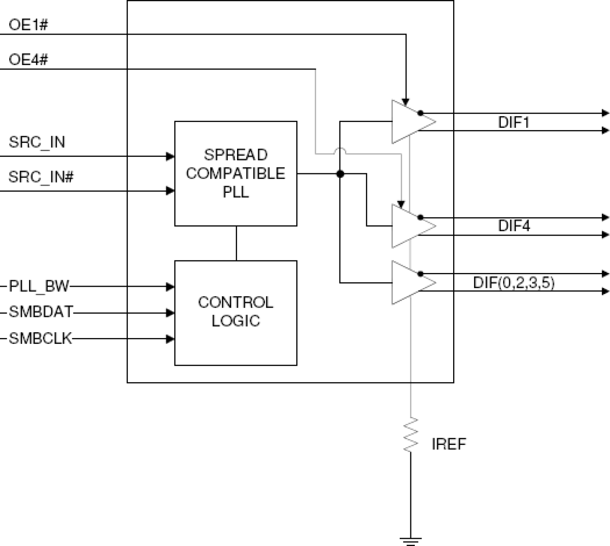
- 6 - 0.7 V current mode differential HCSL output pairs
- Cycle-to-cycle jitter < 50 ps
- Output-to-output skew < 50 ps
- PCIe Gen3 phase jitter < 1.0 ps RMS
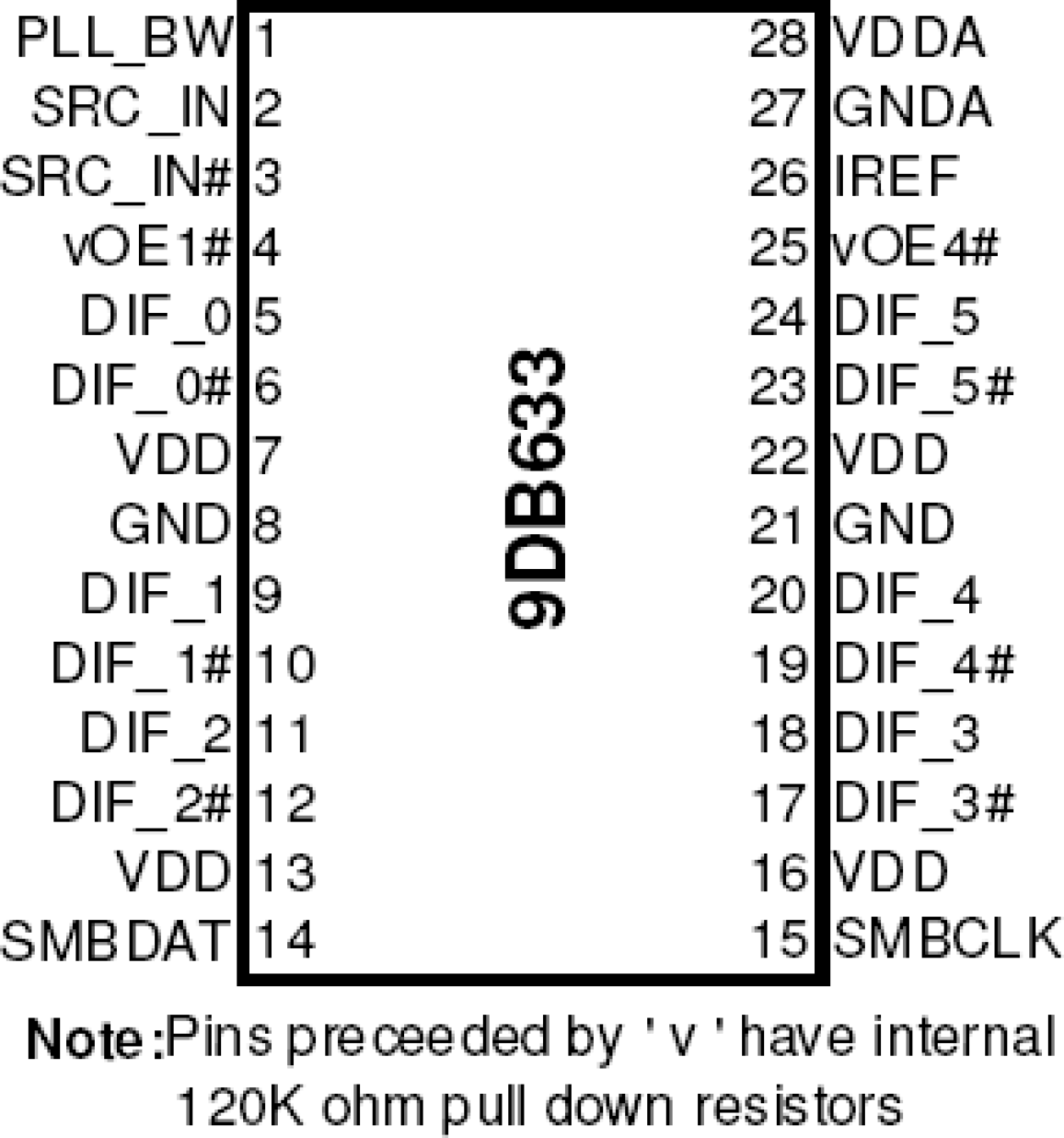
- OE# pins/Suitable for Express Card applications
- PLL or bypass mode/PLL can dejitter incoming clock
- Selectable PLL bandwidth/minimizes jitter peaking in downstream PLL's
- Spread Spectrum Compatible/tracks spreading input clock for low EMI
- SMBus Interface/unused outputs can be disabled
Description
The 9DB633 zero-delay buffer supports PCIe Gen3 requirements, while being backwards compatible to PCIe Gen2 and Gen1. The 9DB633 is driven by a differential SRC output pair from an IDT 932S421 or 932SQ420 or equivalent main clock generator. It attenuates jitter on the input clock and has a selectable PLL bandwidth to maximize performance in systems with or without Spread-Spectrum clocking. An SMBus interface allows control of the PLL bandwidth and bypass options, while 2 clock request (OE#) pins make the 9DB633 suitable for Express Card applications.
Parameters
| Attributes | Value |
|---|---|
| Diff. Outputs | 6 |
| Diff. Output Signaling | HCSL |
| Output Freq Range (MHz) | 10 - 110 |
| Diff. Inputs | 1 |
| Diff. Input Signaling | HCSL |
| Accepts Spread Spec Input | Yes |
| Power Consumption Typ (mW) | 442 |
| Supply Voltage (V) | 3.3 - 3.3 |
| Output Type | HCSL |
| Diff. Termination Resistors | 24 |
| Package Area (mm²) | 42.7 |
| Battery Backup | No |
| Battery Seal | No |
| CPU Supervisory Function POR | No |
| Crystal Frequency Trimming | No |
| Frequency Out Pin | No |
| Inputs (#) | 1 |
| Input Freq (MHz) | 100 |
| Function | Zero Delay Buffer |
| Input Type | HCSL |
| Output Banks (#) | 1 |
| Core Voltage (V) | 3.3 |
| Output Voltage (V) | 3.3 |
| Product Category | PCI Express Clocks |
Package Options
| Pkg. Type | Pkg. Dimensions (mm) | Lead Count (#) | Pitch (mm) |
|---|---|---|---|
| TSSOP | 9.7 x 4.4 x 1.0 | 28 | 0.65 |
Applied Filters:


