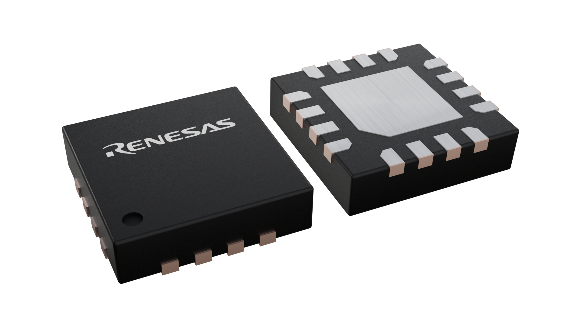

Package Information
| CAD Model: | View CAD Model |
| Pkg. Type: | VFQFPN |
| Pkg. Code: | NLG16 |
| Lead Count (#): | 16 |
| Pkg. Dimensions (mm): | 3.0 x 3.0 x 1.0 |
| Pitch (mm): | 0.5 |
Environmental & Export Classifications
| Moisture Sensitivity Level (MSL) | 3 |
| Pb (Lead) Free | Yes |
| ECCN (US) | EAR99 |
| HTS (US) | 8542.39.0090 |
Product Attributes
| Lead Count (#) | 16 |
| Carrier Type | Tray |
| Moisture Sensitivity Level (MSL) | 3 |
| Qty. per Reel (#) | 0 |
| Qty. per Carrier (#) | 624 |
| Pb (Lead) Free | Yes |
| Pb Free Category | e3 Sn |
| Temp. Range (°C) | -40 to 85°C |
| Additive Phase Jitter Typ RMS (fs) | 27 |
| Additive Phase Jitter Typ RMS (ps) | 0.027 |
| Adjustable Phase | No |
| Advanced Features | Mux/Demux with loopback |
| Channels (#) | 2 |
| Core Voltage (V) | 2.5V, 3.3V |
| Function | Buffer, Multiplexer |
| Input Freq (MHz) | 2500 |
| Input Type | CML, LVDS, LVPECL |
| Inputs (#) | 3 |
| Length (mm) | 3 |
| MOQ | 624 |
| Output Banks (#) | 2 |
| Output Freq Range (MHz) | 2500 |
| Output Type | LVPECL |
| Output Voltage (V) | 2.5V, 3.3V |
| Outputs (#) | 3 |
| Package Area (mm²) | 9 |
| Pitch (mm) | 0.5 |
| Pkg. Dimensions (mm) | 3.0 x 3.0 x 1.0 |
| Pkg. Type | VFQFPN |
| Product Category | Clock Buffers & Drivers, Clock Multiplexers, RF Buffers |
| Requires Terms and Conditions | Does not require acceptance of Terms and Conditions |
| Supply Voltage (V) | 2.5 - 2.5, 3.3 - 3.3 |
| Tape & Reel | No |
| Thickness (mm) | 1 |
| Width (mm) | 3 |
Resources for 853S54I-01
Description
The 853S54I-01 is a 2:1/1:2 Multiplexer. The 2:1 Multiplexer allows one of 2 inputs to be selected onto one output pin and the 1:2 MUX switches one input to one of two outputs. This device may be useful for multiplexing multi-rate Ethernet PHYs which have 100Mbit and 1000Mbit transmit/receive pairs onto an optical SFP module which has a single transmit/receive pair. A 3RD mode allows loop back testing and allows the output of a PHY transmit pair to be routed to the PHY input pair. For examples, please refer to the Application Block diagrams on pages 2-3 of the data sheet. The 853S54I-01 is optimized for applications requiring very high performance and has a maximum operating frequency in 2.5GHz. The device is packaged in a small, 3mm x 3mm VFQFN package, making it ideal for use on space-constrained boards.