
| CAD Model: | View CAD Model |
| Pkg. Type: | TSSOP |
| Pkg. Code: | EJG24 |
| Lead Count (#): | 24 |
| Pkg. Dimensions (mm): | 7.8 x 4.4 x 1.0 |
| Pitch (mm): | 0.65 |
| Moisture Sensitivity Level (MSL) | 1 |
| Pb (Lead) Free | Yes |
| ECCN (US) | EAR99 |
| HTS (US) | 8542.39.0090 |
| Lead Count (#) | 24 |
| Carrier Type | Reel |
| Moisture Sensitivity Level (MSL) | 1 |
| Qty. per Reel (#) | 2500 |
| Qty. per Carrier (#) | 0 |
| Pb (Lead) Free | Yes |
| Pb Free Category | e3 Sn |
| Temp. Range (°C) | -40 to 85°C |
| Core Voltage (V) | 3.3 |
| Feedback Input | No |
| Input Freq (MHz) | 15.313 - 27.2 |
| Input Type | Crystal, LVCMOS |
| Inputs (#) | 2 |
| Length (mm) | 7.8 |
| MOQ | 2500 |
| Output Banks (#) | 2 |
| Output Freq Range (MHz) | 61.25 - 85, 98 - 226.67, 245 - 340, 490 - 680 |
| Output Skew (ps) | 75 |
| Output Type | LVDS |
| Output Voltage (V) | 3.3 |
| Outputs (#) | 3 |
| Package Area (mm²) | 34.3 |
| Phase Jitter Typ RMS (ps) | 0.53 |
| Pitch (mm) | 0.65 |
| Pkg. Dimensions (mm) | 7.8 x 4.4 x 1.0 |
| Pkg. Type | TSSOP |
| Product Category | FemtoClock, Low Jitter Clocks (<700 fs RMS) |
| Prog. Clock | No |
| Reel Size (in) | 13 |
| Reference Output | No |
| Requires Terms and Conditions | Does not require acceptance of Terms and Conditions |
| Spread Spectrum | No |
| Tape & Reel | Yes |
| Thickness (mm) | 1 |
| Width (mm) | 4.4 |
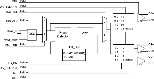
The 844003BI-01 is a 3 differential output LVDS synthesizer designed to generate Ethernet reference clock frequencies. Using a 19.53125MHz or 25MHz, 18pF parallel resonant crystal, the following frequencies can be generated based on the settings of 4 frequency select pins (DIV_SELA[1:0], DIV_SELB[1:0]): 625MHz, 312.5MHz, 156.25MHz, and 125MHz. The 844003BI-01 has 2 output banks, Bank A with 1 differential LVDS output pair and Bank B with 2 differential LVDS output pairs.
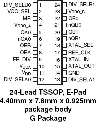
The two banks have their own dedicated frequency select pins and can be independently set for the frequencies mentioned above. The 844003BI-01 uses our 3rd generation low phase noise VCO technology and can achieve 1ps or lower typical rms phase jitter, easily meeting Ethernet jitter requirements. The 844003BI-01 is packaged in a small 24-pin TSSOP package.