TOKYO, Japan ― Renesas Electronics Corporation (TSE:6723), a premier supplier of advanced semiconductor solutions, and Hitachi, Ltd. (TSE: 6510) today announced a technology collaboration to enable continuous-time digital calibration of a delta-sigma (ΔΣ) modulator and an analog-to-digital (A/D) converter circuit.
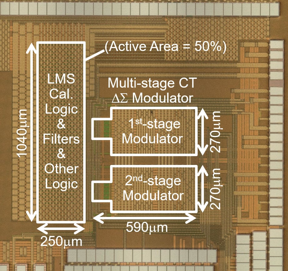
Designed to boost the performance of ΔΣ A/D converters for stable performance under the harsh conditions required for automotive semiconductor devices, the new technology comprises (1) enhanced precision by using a least mean square (LMS) algorithm to measure and calibrate the transfer function of a continuous-time ΔΣ modulator, and (2) the world’s first multi-rate LMS search algorithm, which lowers the order and operating frequency of the coefficient search circuit and FIR digital filter to reduce power consumption. The 28 nm process was used to implement a multi-stage ΔΣ A/D converter employing sequential integrators operating at high speed.
Previously, digital calibration circuits were required to operate at an oversampling frequency of A/D converters, but the new circuit reduces the operating frequency to one-fourth the previous frequency. As a result, high-speed, high-precision operation with a signal bandwidth of 15 MHz and dynamic range of 74.3 dB is achieved when operating at an oversampling frequency of 480MHz. By reducing the digital calibration circuit operating frequency to 120MHz, low-power operation is also achieved, with 37mW power consumption (analog:19mW, digital:18mW). In addition, the new technology has been confirmed to provide stable performance over a wide temperature range, proving that it is highly robust and capable of stable operation under punishing conditions (note 1).
The results of this joint effort with Hitachi were presented by Renesas on February 18 at the International Solid-State Circuits Conference (ISSCC) 2020.
In recent years, as advanced driver assistance systems (ADAS) and self-driving vehicles come closer to becoming a reality, there has been an increasing need for automobiles to incorporate a variety of sensors, such as millimeter wave radar, LiDAR, and ultrasonic wave sensors, in order to detect objects and people, and to provide an awareness of the vehicle’s surroundings. A/D converters used to convert analog signals from such sensors into digital signals must operate at a high speed and with high precision. However, the harsh conditions specific to automotive vehicles have made obtaining stable performance an important issue. In response, Renesas and Hitachi developed the new continuous-time digital calibration technology to make high-speed, high-precision ΔΣ A/D converters capable of withstanding punishing conditions a reality. The new A/D converter circuit technology developed jointly by Renesas and Hitachi is described below.
(1) Technology using LMS algorithm to measure and calibrate the transfer function of a continuous time ΔΣ modulator
Generally, RC integrators that do not require input sampling capacitor and are suitable for high bandwidth are employed as a method of increasing the conversion speed of the ΔΣ A/D converter. These integrators are connected in cascade for a high-order loop filter. However, when the input is excessively large, precision is lost due to the ΔΣ modulators’ oscillation. On the other hand, a multi-stage ΔΣ modulator consisting of low-order ΔΣ modulators connected in multiple stages can be used to achieve a higher-order ΔΣ modulator while maintaining the stability of the ΔΣ A/D converter. However, in a multi-stage configuration, precision suffers if the analog transfer functions and digital transfer functions do not match perfectly, and for this reason such configurations are susceptible to environmental variations such as changes in temperature, making it difficult to achieve higher precision.
To solve the difficulty in achieving higher precision, typical of multi-stage ΔΣ modulators, which are extremely stable, Renesas and Hitachi jointly developed a technology that digitally calibrates the transfer function of the ΔΣ modulator. This technology inputs a pseudo-random number signal to the quantizer-input of the first-stage ΔΣ modulator as a reference signal, which makes background search possible using an LMS algorithm of the first-stage modulator’s noise transfer function and the second-stage modulator’s signal transfer function at the same time. The coefficients searched by the LMS algorithm are input to FIR digital filters, and the second-stage modulator result is used to completely cancel the quantization error of the first-stage modulator, making it possible to obtain high-precision A/D conversion results. This new technology enables calibration within the digital circuits operating in the background even if the characteristics of the analog integrators are affected by environmental variations such as temperature changes. As a result, Renesas and Hitachi succeeded in achieving both high precision and robustness in a highly stable multi-stage ΔΣ modulator, something previously considered difficult if not impossible.
(2) World’s first multi-rate LMS search algorithm that enables smaller circuit scale and low power consumption
When searching ΔΣ modulator transfer functions using the LMS-based coefficient search algorithm described above, the number of tap coefficients required by the FIR digital filter was very large (more than 100) when the gain-bandwidth product of the integrator amplifier circuit was insufficient, which meant that the scale of the logic circuits would be impracticably large. However, it was found that extracting only the transfer function characteristics near the signal bandwidth was sufficient for transfer function calibration. By reducing unnecessary frequency information by means of a post-conditioner, it became possible to substantially reduce the number of tap coefficients, even when the gain-bandwidth product of the amplifier circuit was small. In addition, by using shift registers to store reference signal data, Renesas and Hitachi developed a new calibration circuit using an LMS algorithm that was not affected by sub-sampling. This made it possible to reduce the operating frequencies of the coefficient search and FIR filter to one-fourth what they previously were. The world’s first digital calibration circuit technology successfully reduced the circuit scale while also reducing power consumption (Note 2).
Renesas will continue to develop practical applications for this technology to enable high-speed, high-precision, and highly reliable A/D conversion of automotive sensor signals in order to accelerate the widespread adoption of self-driving technology and the realization of a safer and more secure driving experience.
Notes
1. The characteristics of the A/D converter on the test chip confirm that, within a temperature range of −20 to 125°C, the transfer function coefficient search achieves the background operation and with a SNR variation of no more than ±1 dB.
2. In the new A/D converter, the number of FIR filter tap coefficients required when the gain-bandwidth product of the integrator amplifier circuit is insufficient is reduced to 10 compared to well over 100 using the conventional method.
About Renesas Electronics Corporation
Renesas Electronics Corporation (TSE: 6723) delivers trusted embedded design innovation with complete semiconductor solutions that enable billions of connected, intelligent devices to enhance the way people work and live. A global leader in microcontrollers, analog, power, and SoC products, Renesas provides comprehensive solutions for a broad range of automotive, industrial, infrastructure, and IoT applications that help shape a limitless future. Learn more at renesas.com. Follow us on LinkedIn, Facebook, Twitter, and YouTube.
(Remarks) All registered trademarks or trademarks are the property of their respective owners.
The content in the press release, including, but not limited to, product prices and specifications, is based on the information as of the date indicated on the document, but may be subject to change without prior notice.