特長
- 4 - 0.7 V current mode differential HCSL output pairs
- 1 - 3.3 V LVTTL REF output
- Pin-to-Pin with 9FG104D/Easy upgrade to PCIe Gen3
- Generates common frequencies from 14.318 MHz or 25 MHz; single part supports multiple applications
- Provides copy of reference output; eliminates need for additional crystal or oscillator
- Unused outputs may be disabled in Hi-Z save system power
- Device may be configured by SMBus and/or strap pins; can be used in systems without SMBus
- Cycle-to-cycle jitter: < 50 ps with 25 MHz input
- Output-to-output skew: <50 ps
- Phase jitter: PCIe Gen3 < 1 ps RMS
- Phase jitter: QPI 9.6 GB/s < 0.2 ps RMS
- 10 ppm synthesis error with 25 MHz input and Spread Off
説明
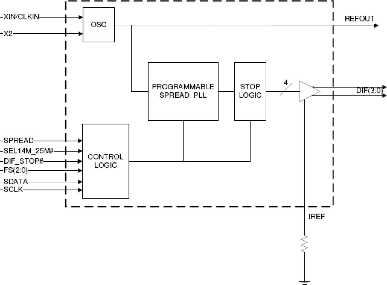
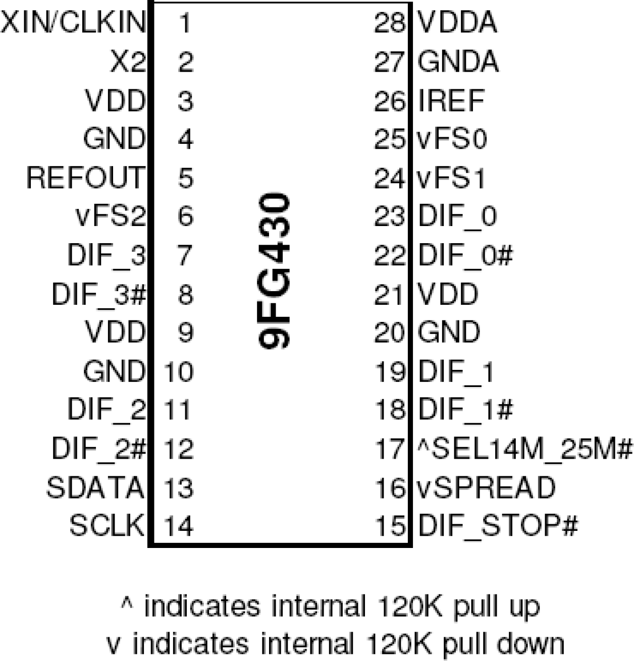
The 9FG430 is a Frequency Timing Generator that provides 4 HCSL differential output pairs. These outputs support PCI-Express Gen3, and QPI applications. The part supports Spread Spectrum and synthesizes several additional output frequencies from either a 14.31818 MHz crystal, a 25 MHz crystal or reference input clock. The 9FG430 also outputs a copy of the reference clock. Complete control of the device is available via strapping pins or via the SMBus interface.
適用されたフィルター


