Features
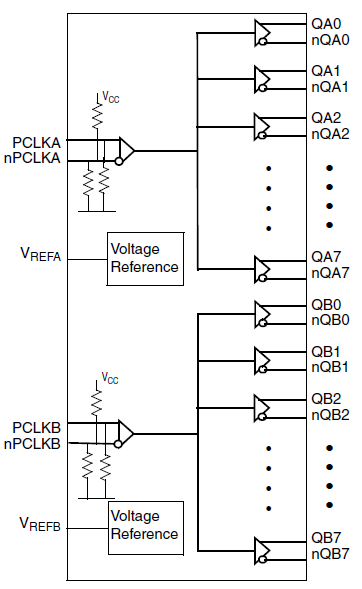
- Two 1:8, low skew, low additive jitter LVPECL fanout buffers
- Two differential clock inputs
- Differential PCLKA, nPCLKA and PCLKB, nPCLKB pairs can accept the following differential input levels: LVDS, LVPECL, CML
- Differential PCLKA, nPCLKA and PCLKB, nPCLKB pairs can also accept single-ended LVCMOS levels.
- Maximum input clock frequency: 2GHz
- Output bank skew: 15ps (typical)
- Propagation delay: 390ps (maximum)
- Low additive phase jitter, RMS: 54fs (maximum) (fREF = 156.25MHz, VPP = 1V, 12kHz to 20MHz, VCC = 3.3V)
- Full 3.3V and 2.5V supply voltage
- Maximum device current consumption (IEE): 143mA
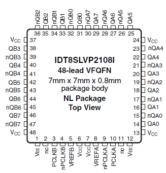
- Available in a Lead-free (RoHS 6), 48-lead VFQFN package
- -40 °C to 85 °C ambient operating temperature
Description
The 8SLVP2108I is a high-performance differential dual 1:8 LVPECL fanout buffer designed for the fanout of high-frequency, very-low additive phase noise clock and data signals. The 8SLVP2108I is characterized for operation from a 3.3V or 2.5V power supply. Guaranteed output-to-output and part-to-part skew characteristics make the 8SLVP2108I ideal for those clock distribution applications demanding well-defined performance and repeatability. Two independent buffers with eight low-skew outputs each are available. The integrated bias voltage references enable easy interfacing of single-ended signals to the device inputs. The device is optimized for low power consumption and low additive phase noise.
Parameters
| Attributes | Value |
|---|---|
| Outputs (#) | 16 |
| Inputs (#) | 2 |
| Channels (#) | 2 |
| Input Freq (MHz) | - |
| Output Freq Range (MHz) | - |
| Output Skew (ps) | 25 |
| Adjustable Phase | No |
| Noise Floor (dBc/Hz) | -162 |
| Additive Phase Jitter Typ RMS (fs) | 43 |
| Output Type | LVPECL |
| Supply Voltage (V) | - , - |
| Advanced Features | Dual Buffer |
Package Options
| Pkg. Type | Pkg. Dimensions (mm) | Lead Count (#) | Pitch (mm) |
|---|---|---|---|
| VFQFPN | 7.0 x 7.0 x 0.9 | 48 | 0.5 |
Application Block Diagrams

|
eCPRI Mass MIMO for RRU
eCPRI MIMO RRU with low phase noise, deterministic latency, and high timing precision for 5G networks.
|
Applied Filters:
Filters
Software & Tools
Sample Code
Simulation Models
Description
Overview of IDT's 8LSVP (LVPECL) and 8SLVD (LVDS) families of low-jitter fanout buffers from IDT. Fanout buffers are a useful building block of many clock trees, providing signal buffering and multiple low-skew copies of the input signal. IDT's high-performance, low additive phase noise, differential clock fan-out buffers offer up to 2 GHz clock operation, low additive phase jitter (12kHz - 20MHz) of 50 to 100 femtoseconds RMS max, fast output rise & fall times (less than 150ps), and single and dual channel functions (dual: matched propagation delay). Presented by Baljit Chandhoke, Product Marketing Manager at Integrated Device Technology, Inc. To learn more about IDT's industry-leading portfolio of fanout buffers, visit Renesas's RF Buffer page.
Transcript


