特長
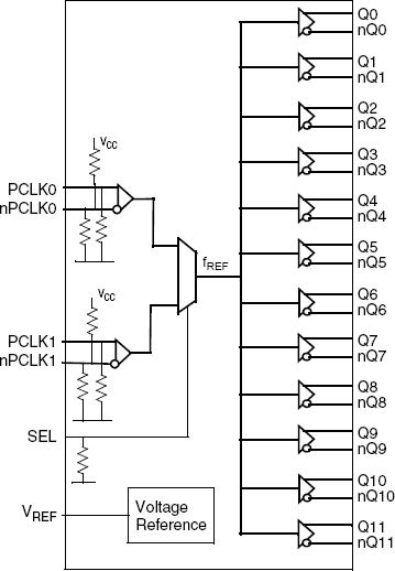
- Twelve low skew, low additive jitter LVPECL outputs
- Two selectable, differential clock inputs
- Differential pairs can accept the following differential input levels: LVDS, LVPECL, CML
- Maximum input clock frequency: 2GHz
- LVCMOS interface levels for the control input (input select)
- Output skew: 15ps (typical)
- Propagation delay: 550ps (maximum)
- Low additive phase jitter, RMS: <50fs (typical)
- Full 3.3V and 2.5V supply voltage
- Device current consumption (IEE): 118mA (typical)
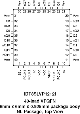
- Available in Lead-free (RoHS 6), 40-Lead VFQFN package
- -40°C to 85°C ambient operating temperature
説明
The 8SLVP1212I is a high-performance, 12 output differential LVPECL fanout buffer. The device is designed for the fanout of high-frequency, very low additive phase-noise clock and data signals. The 8SLVP1212I is characterized to operate from a 3.3V and 2.5V power supply. Guaranteed output-to-output and part-to-part skew characteristics make the 8SLVP1212I ideal for those clock distribution applications demanding well-defined performance and repeatability. Two selectable differential inputs and twelve low skew outputs are available. The integrated bias voltage generators enables easy interfacing of single-ended signals to the device inputs. The device is optimized for low power consumption and low additive phase noise.
パラメータ
| 属性 | 値 |
|---|---|
| Outputs (#) | 12 |
| Inputs (#) | 2 |
| Channels (#) | 1 |
| Input Freq (MHz) | - |
| Output Freq Range (MHz) | - |
| Output Skew (ps) | 15 |
| Adjustable Phase | No |
| Noise Floor (dBc/Hz) | -160 |
| Additive Phase Jitter Typ RMS (fs) | 45 |
| Output Type | LVPECL |
| Supply Voltage (V) | - , - |
パッケージオプション
| Pkg. Type | Pkg. Dimensions (mm) | Lead Count (#) | Pitch (mm) |
|---|---|---|---|
| VFQFPN | 6.0 x 6.0 x 0.9 | 40 | 0.5 |
適用されたフィルター
フィルター
ソフトウェア/ツール
サンプルコード
シミュレーションモデル
Description
Overview of IDT's 8LSVP (LVPECL) and 8SLVD (LVDS) families of low-jitter fanout buffers from IDT. Fanout buffers are a useful building block of many clock trees, providing signal buffering and multiple low-skew copies of the input signal. IDT's high-performance, low additive phase noise, differential clock fan-out buffers offer up to 2 GHz clock operation, low additive phase jitter (12kHz - 20MHz) of 50 to 100 femtoseconds RMS max, fast output rise & fall times (less than 150ps), and single and dual channel functions (dual: matched propagation delay). Presented by Baljit Chandhoke, Product Marketing Manager at Integrated Device Technology, Inc. To learn more about IDT's industry-leading portfolio of fanout buffers, visit Renesas's RF Buffer page.
Transcript


