Features
- Low voltage single supply operation: VDD = 1.8V to 5.5V
- Low input offset voltage: VIO ≤ ±6.0mV
- Low input bias current: IB ≤ (1pA)
- Wide output voltage range: VOUT : VSS+0.1V to VDD-0.1V (at Io = 1mA)
- Supply current (per channel) : IDD = 40μA typical
- High slew rate: SR = 0.35V/μs typical
Description
The READ4303G is input and output full range quad CMOS Operational Amplifier realizing low voltage and low current consumption operation. This IC can be used in minimum operating supply voltage from 1.8V, and in wide ambient temperature range from -40˚C to +105˚C.
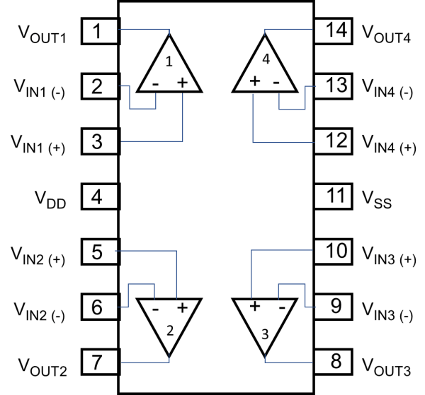
Available in 14 pin TSSOP.
Parameters
| Attributes | Value |
|---|---|
| Channels (#) | 4 |
| Temp. Range (°C) | -40 to +105 |
| Bandwidth (MHz) | 0.55 |
| Gain Min | 60dB |
| Offset Voltage (Max) (mV) | 6 |
| IBIAS (nA) | 0.001 |
| CMRR (dB) | 80 |
| Rail-to-Rail Input | Yes |
| Rail-to-Rail Output | Yes |
| Common Mode Input Voltage Range (V) | 0.3 - 6.5 |
| Output Voltage Swing Range (V) | VDD+0.1 - VSS+0.1 |
| IS per Amp (mA) | 0.04 |
| Single Supply Voltage Range (V) | 0.3 - 6.5 |
| Slew Rate (V/µs) | 0.35 |
| VS (Min) (V) | 0.3 |
| VS (Max) (V) | 6.5 |
| Topology [Rail 1] | - |
| Enable | - |
| Input Offset Voltage Vio (Max) (mV (±)) | 6 |
| Supply Current Icc/Idd (Max) (mA) | 0.04 |
| Qualification Level | Standard |
| Simulation Model Available | SPICE |
Package Options
| Pkg. Type | Lead Count (#) | Pitch (mm) |
|---|---|---|
| TSSOP | 14 | 0.65 |