Features
- Gain bandwidth product: 4.0GHz
- Input voltage noise: 0.85nV/√(Hz)
- Differential slew rate: 5,600V/µs
- 2VP-P, 2-tone IM3 (200Ω) 100MHz: -109dBc
- Supply voltage range: 3.0V to 4.2V
- Quiescent power (3.3V supply): 115mW
Description
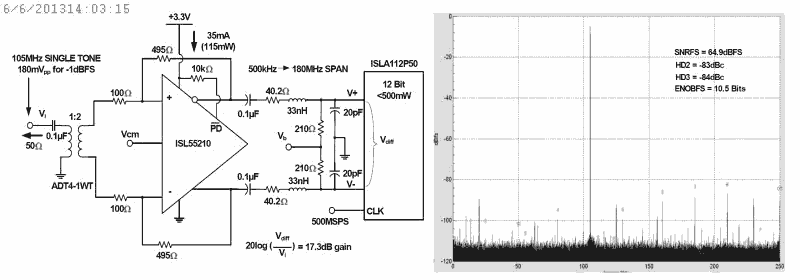
The ISL55210 is a very wide band, fully differential amplifier (FDA) intended for high dynamic range ADC input interface applications. This voltage feedback FDA design includes an independent output common mode voltage control. At the lowest quiescent power (115mW), the ISL55210 offers a 4.0GHz gain bandwidth product with a very low input noise of 0.85nV/√(Hz). In a balanced differential I/O configuration, with 2VP-P output into a 200Ω load configured for a gain of 15dB, the IM3 terms are <-100dBc through 110MHz. With a minimum operating gain of 2V/V (6dB), the ISL55210 supports a wide range of higher gains with minimal BW or SFDR degradation. Its ultra-high differential slew rate of 5,600V/µs ensures clean large signal SFDR performance or a fast settling step response. The ISL55210 requires only a single 3.3V (max 4.2V) power supply with a 35mA typical quiescent current. This industry-leading low-current solution can be further reduced when needed using the optional power shutdown to <0.4mA supply current. External feedback and gain setting resistors give maximum flexibility and accuracy. A companion device, the ISL55211, includes on-chip feedback and three possible gain setting connections where an internally fixed gain solution is preferred. The ISL55210 is available in a leadless, 16 Ld TQFN package and is specified for operation over the -40 °C to +85 °C ambient temperature range.
Parameters
Attributes | Value |
---|---|
Channels (#) | 1 |
Temp. Range (°C) | -40 to +85°C |
Bandwidth (MHz) | 2200 |
Gain Min | 2 |
Offset Voltage (Max) (mV) | 1.4 |
IBIAS (nA) | 50000 |
IOUT (A) | 0.045 |
CMRR (dB) | 75 |
PSRR (db) | 90 |
Rail-to-Rail Input | No |
Rail-to-Rail Output | No |
IS per Amp (mA) | 35 |
Noise VN (nV/√Hz) | 0.85 |
Single Supply Voltage Range (V) | - |
Slew Rate (V/µs) | 5600 |
VOUT (V) | 3.8 |
VS (Min) (V) | 3 |
VS (Max) (V) | 4.2 |
2nd Harmonic (dB) | -105 |
3rd Harmonic (dB) | -120 |
AVOL (dB) | 100 |
Topology [Rail 1] | FDA |
Enable | Yes |
Output Headroom (V) | 1 |
Distortion Conditions | 2Vpp, 20MHz |
Qualification Level | Standard |
Package Options
Pkg. Type | Pkg. Dimensions (mm) | Lead Count (#) | Pitch (mm) |
---|---|---|---|
TQFN | 3.0 x 3.0 x 0.75 | 16 | 0.5 |
Applications
- Low power, high dynamic range ADC interfaces
- Differential mixer output amplifiers
- SAW filter pre/post driver
- Differential Comms-DAC output drivers
Applied Filters:
Filters
Software & Tools
Sample Code
Simulation Models
This video demonstrates some wideband single ended input to differential output options using the ISL55210 Active Balun Evaluation Platform.
Transcript
Today we're going to be discussing a new circuit technique that we've developed as part of our ISL55210. That's a very wide band, 4GHz fully differential amplifier that includes features internally that are unique to that device in the industry.
So we'll start today by looking at the legacy approaches of going from single differential, first starting with a fully differential amplifier, which has been an emerging component of the industry. It's been extremely useful for signal path processing and ADC driving. So here we see, a typical circuit that you would find in lots of suppliers' datasheets that are supplying high performance, fully differential amplifiers or FDAs, where we're trying to provide an input match to a source impedance, and gain from that matching input impedance, to a differential output swing.
Typically, what you'll see, is you'll see a circuit with a resister to ground. I call that RT for termination resister. We don't have to have a blocking cap for DC coupled for all these applications, but for simplicity here, we'll use a blocking cap, since we're comparing this to a balun approach which is necessarily AC coupled.
So we'll see resister to ground which is part of our input termination resistance and we'll typically see a resister going to the summing junction, then two equal feedback resisters will comprise the circuit. What we're trying to do with these elements is we're trying to get a 50ohm input match here, and then balance the divider equations going back to each side. So, you'll notice if you look at the impedance past the cut off frequency as a blocking capacitor, if you notice the impedance looking back each way, we'll see that it's matched. That's necessary for the differential balance.
But if you look at this circuit for just a moment, you wonder what's going on with this? We're trying to get a 50ohm input match, and that's clearly not the case looking at these two resisters. What's going on is with a fully differential amplifier as a single ended input signal moves up and down, the common mode voltage on the inputs have to move, to satisfy the common mode loop which is trying to hold the average voltage constant.
Internal to a part like the ISL55210, which would be our feature part today, we have a common mode reference voltage that defaults to 1.2V. This circuit incidentally is coming from our free online simulator that you can download and run any of the circuits I'm showing you today in a simulation package, available free from Renesas.
The ISL55210 has a model in that package that reflects all the features we're trying to describe today.
So, it is possible to hit a designed target. This is the solution for the resister to ground. All of these active termination kind of circuits, end up with a quadratic solution. Once you get this value having selected a feedback resister that's appropriate for the device you're using, a target gain and a source impedance that you're trying to match, this will give you the solution for the termination resister to ground. From that, you can get the other two resisters from these simple equations. If we can get rid of this resister, and just have the match going into the inverting summing junction, we'll find that the noise goes way down on this circuit which will always be the case if you don't throw a signal away into a terminating element to ground.
So let's go next just to some other ways of doing the single differential using a FDA.
This video demonstrates other ways of doing the signal to differential using an FDA with the ISL55210 Active Balun Evaluation Platform.
Transcript
Hello, this is Michael Steffes, the Senior Applications Manager for Renesas' high-speed signal path products. And today we're going to continue our discussion on how to get single to differential conversion in a couple different techniques for your circuits.
Showing on the screen behind me is a very capable technique of using an input balun and a fully-differential amplifier, which has been a very useful technique over the past decade. We're going to move forward from this, of course, to show an active balun approach using the ISL55210. But it's this circuit that you would get on the ISL55210 evaluation board available from Renesas' website or your favorite distributor.
This circuit comes with an input transformer and then an output transformer, really just for measurement purposes. On the input side, we use a range of transformers or baluns to get from single to differential into a termination impedance being set here by the gain resistors. So this is a very nice circuit and it certainly works very well as a low-power, single differential circuit. Once we're balanced on the opposite side, this circuit does have some advantages in terms of second harmonic suppression.
Now, if we move on to this new technique enabled by the ISL55210, we eliminate both the balun, and in this case, we eliminate the resistor to ground that you'll see in everybody else's fully-differential amplifier datasheets or application notes. And we're going to try to do our input match and gain setting just with the resistors we have available in the circuit. If we do that and run a sweep of gains, we can step the gain up from 14dB to 34dB, and see what happens to the resistor values.
One of the really surprising things for instance, at a gain of 20, let's just look at these values, is the input resistor that we end up driving is an extremely low value, 4.57ohm. But the circuit will appear as if it's giving you a 50ohm input match through very broad frequencies. A couple things come out of that, what we're seeing here is that the input match is largely being set by the action of the common-mode loop because that's what's giving us our active termination characteristic. And to hold that match through extremely high frequencies implies you need a very broadband common-mode loop which is one of the unique characteristics of the ISL55210 is it has a common-mode loop band with an exceeding 1.5GHz, whereas, all other FDAs today have a much lower bandwidth on the common-mode loop.
As we look at these extremely low resistor values, we would expect the noise, or the input-referred noise figure, to step down considerably using these 4.5ohm kind of input resistors in the active balun circuit. You can go to another video to see those test results.
This video discusses the ISL55210 Active Balun Evaluation Platform's test results for frequency response and measured noise.
Transcript
Hello, this is Michael Steffes, Senior Applications Manager for High-Speed Signal Path at Renesas. Today we'll continue our discussion on this active balun approach of using a wide band for differential amplifier, the ISL55210.
And so what we are going to do now is we are going to look at detail at the frequency response and the measured noise figure for a couple of configurations of this very flexible approach to getting a input impedence match with broadband single to differential gain with no actual magnetics in the circuit.
So what we show on the screen here is the configuration of the circuit as the board would be delivered of our active balun evaluation board, would be delivered in this configuration on the screen. We actually have three different output interface options. Here we are showing a transmission line balun, which actually gives quite a bit broader frequency response flatness then a more typical flux couple balun but that option is also available on the board.
So if we look at this circuit, we configured it for a 50ohm input match. We've got a 16.4dB gain to the output pans. And we're going to take a 6dB loss in the matching and we are estimating about a .2dB to .4dB insertion loss in the balun. Now that’s not modeled here but we will see it on the measurement of the board.
So let’s run the simulation and we will measure the output all the way through to the final 50ohm load. We should see a response shape that looks something like this. It does simulate at about 10.4dB. Let’s look closely at where we would see about a .5dB roll off from 10.4. So that is going to be 9.9. We should expect to see a .5dB flatness with the higher frequencies, up through about 470MHz is what the simulations would predict. So this is what we would expect to see.
Let’s go over to the network analyzer and see what we really get. We've got our evaluation board configured to measure the response shape. The marker is currently at 10MHz and we see about a 10.2dB measured gain to the max load. And let’s go up in frequency and just see where we start to see a deviation and that is going to happen at about 470MHz, very much like our simulations.
Extremely capable circuit. Let’s go back now and look at our noise performance for this type of circuit. We will go to a little higher gain to check the noise. And if we do that we will use this table and we will see that we need about a 4.60ohm input resister to get a 50ohm match. We'll need about a 543ohm feedback resister on each side. And we should be getting about 450MHz bandwidth in that configuration. So if we configure that active balun board and with those resister values, we can go make a measurement of the input noise figure for a couple different configurations. This green curve we are showing on this comparison plot was actually in the standard configuration with a resister to ground, 110ohm that typically you would see in these kind of circuits. And we can see, it gives about a 10dB noise figure when you get up above the 50MHz region.
If we now do the same input impedance and the same gain setting, but eliminate the resister ground. Completely depending on the current mode loop band to get our match. We'll see the noise figure indeed drop significantly. Down into the 7dB noise figure region. That correlates to approximately a .9nV input preferred noise. And since the ISL55210 has already a .85nV device, this essentially shows that the resister noise contribution using this active balun approach are extremely low. We've essentially taken the resister noise out of the performance of the circuit.
If you like to try these circuits for yourself and measure these noise in different configurations, go on the Renesas website and order the active balun evaluation board, where there is also an application note describing the board.
The demo concludes for the ISL55210 Active Balun Evaluation Platform and discusses input impedance match.
Transcript
Hello, this is Michael Steffes, Senior Applications Manager for high-speed signal path products at Renesas. And we're gonna conclude our series on the active balun approach of using the ISL55210 to get a very broadband single to differential conversion. We've already seen that it gives an extremely flat frequency response through 500MHz. But does it really give a good input impedance match, as the equations would predict?
Turning to a very venerable piece of equipment, the HP or Agilent 4195, we've configured this box with one of our active balun boards to measure the input impedance here. So we've done a calibration from 1MHz to 500MHz, in an S1 one calibration, to measure the input impedance. If we look over that span, the board is powered, and we are taking a measurement, we can trigger it, and we can see that it will update the curves just slightly.
At 10MHz, we're seeing 51ohm, and a minus two degrees, almost perfect match at 10MHz, but continuing and moving out markers up to 500MHz, we'll see that we only deviate up to 53ohm approximately, at 500MHz, and 3.3 degrees. Looking at the magnitudes here, that's better than 30dB return loss over the range of probably about 2MHz to 500MHz. That's a range of input match, just really not supported by any balance. But particularly if you consider we're giving about a 10dB gain to the match load here, which is equivalent to having a turns ratio of about 3.3.
So let's turn back to some of the other characteristics of this circuit, we're obviously are getting a very good input match. So we're trying to emulate a doubly terminated 50ohm environment for output intercept measurement purposes, and that's the purpose of this circuit.
The next step in our intercept measurement, was to come up with an extremely low distortion input signal which we're getting with this pair of power amplifiers, which isolate our signal sources during the measurement process. The test signal coming out here would have the two test tones on them, and we're presenting probably better than a 120dB dynamic range of the source signals, using this approach.
Let's look at our measured data. This is measured using the active balun circuits, set up for a gain of 10dB net to the match load, and a 50ohm input match, that we've discussed previously. Here we’ve got some measured data, and then a fit line, since what we're seeing here is the open loop gain roll off of the ISL55210, up through frequency.
At 200MHz, we're measuring approximately 40dBm to the match load, in a standard output intercept kind of definition. And at 300MHz, we're still above 30dBm. So for a 115mW type device, this is actually exceptional intercept through very high frequencies. The approach certainly works as an IF Amplifier, what else would we use that for?
We could potentially use this in a number of areas, wherever you need a good input match, and of course, it's extremely flexible. If for instance, you need to terminate a cable, and the cable itself is not exactly 50ohm, you can go just go into the equations and put in what you're trying to terminate to, and adjust the resister value to get exact match. So for instance, if you have a cable that needs to be matched, and the cable is not exactly 50ohm, it's 53ohm perhaps, or 55ohm, you can adjust the input resistors to get perfect match over a huge range here.
75ohm systems can be easily be implemented, obviously for cable modem kind of applications. It’s just a very flexible circuit, and wide range of applications.
So go to the Renesas website and order the active balun implementation of the ISL55210, see how you can use it and let us know.
The high-speed ADC evaluation platform enables rapid testing and performance validation of the entire portfolio of low-power 8 to 16-bit, 40 to 500MSPS high performance analog-to-digital converters.
Transcript
Good morning. My name is Michael Steffes, Applications Manager in the High-Speed Amplifier area. This morning, we're demonstrating a new evaluation platform including our high-speed amplifier, the ISL55210 and our 12-bit 500 Mega-Sample ADC.
From Intersil, you would require a motherboard which allows you to test many different kinds of converters. This is available online. On that, we attached two different daughter boards. Normally, we deliver a converter daughter boards with only two transformers. This requires a 10dBm board edge power level but works just fine. What we're demonstrating this morning is a new daughter board which includes an amplifier stage which reduces the board edge power to -10dBm, much more realistic for systems.
So once you get a motherboard, you would download the software which is the converter software - it's a free download - to drive the motherboard through a USB connection and be able to attach on any of the series of daughter boards including the amplifier or different converters.
So go online today and look for each of these elements for your high-performance converter data acquisition needs.
This video demonstrates the platform daughter board that includes both an ISL55210 FDA and an ISLA112P50 12-bit, 500 MSPS ADC.
Transcript
Good morning, this is Micahel Steffes demonstrating our new daughter board that includes both an amplifier and an ADC.
Here we're demonstrating a very capable single-ended to differential signal chain that includes our new 4GHz ISL55210. This is the widest bandwidth, lowest noise, lowest distortion, lowest power FTA solution today. On this board, we have implemented the cleanest single to differential conversion using an input transformer that's the lowest power way to get a single to differential. Since most lab and system sources are single ended, that's extremely useful.
Then the amplifier comes in as a pure differential I/O stage with about 2GHz bandwidth in this configuration. Even though it's the lowest noise device on the market, we have a 2GHz bandwidth at the output and we have to insert the capability for an interstage filter which appears here.
Here we've implemented an AC coupled second order RLC filter that includes the input impedance of the ADC as part of the filter design which is critical in any actual design. This particular implementation is giving us a 180MHz 3dB bandwidth with a second order cut-off but we certainly look forward to working with you on your requirement to tune this up to your specific needs once you have ordered a board from the Renesas website.
This video walks you through the proper set up of your own data acquisition test environment, from the initial signal generator all the way through the data acquisition motherboard. You'll need the daughterboard with the ISL55210 FDA as well as the ISLA112P50 12-bit, 500 MSPS ADC.
Transcript
So now we're gonna show how you actually can demonstrate the level of performance that we're talking about on this ISL55210 plus the ISLA112P50 12-bit 500 mega-sample daughter board. All of this is available to you from the Renesas website, but let's look in detail at what we're doing to get to this, to demonstrate this performance. First of all, of course we have a signal generator, a bandpass filter, we have our ADC board, we have a clock generator, we have our data capture board, and that is driven from our converter software that is a free download from the Renesas website.
Now of course, when we're testing converters, we're usually looking, with single or two-tone testing to illustrate the capability of narrow-band capability of the converter. So we start out with a very low phase noise signal generator, that we show here. Here we're testing at a single tone, 105MHz input frequency. And we're coming out with only a -4dBm power level. Recall in the interface that we're working with, we are providing quite a bit of gain from board edge. So we only are using a -4dBm. Now, what's critical about these test sources, for really showing the capability of the amplifier plus the converter, is that they be very low phase noise sources. Not only do we need a low phase noise on the clock, but we need a low phase noise on the source as well.
The next element in our signal data acquisition evaluation system is of course a filter. While our signal sources are very low phase noise, they're extremely poor harmonic distortion. If we don't cut off all those harmonics, we'll see those in our ADC FFT. So what we're doing here is we're taking the output at 105MHz into a tunable bandpass filter. This particular one that we use is a 65MHz to 125MHz, with a 5% bandwidth. What we're trying to achieve is a single tone output with a narrow noise bandwidth, so that we can expose the full capability of our amplifier plus ADC performance. One additional element we use is an output attenuator, because the output impedance of these filters is not super well-controlled out of band, so we get a little bit better using this attenuator before we hit the amplifier.
So the next element that we require for a lab environment data acquisition test system is a very good clock. Now, here we're using a Crystek 500MHz clock, which has the unique capability of extremely low phase noise. This of course helps us show the SNR capability of the converter. Now that clock is generating a 500MHz clock signal that we then bandpass filter before we drive the ADC. Now on the daughter board itself, we have now a good clock coming in, and a good 105MHz signal coming in. We have a signal here. We're coming in to a transformer that converts our single-ended signal to a differential signal, where we're running the FDA as a differential I/O port. And then on the output side, we've implemented an RLC second-order filter, which also includes a way to tap off our signal for a network analyzer, right at the input to the ADC. So we can actually measure the frequency response up to the converter input in situ.
In a sense we're testing what the frequency response is to the converter, while the converter is operating exactly like it would be in a system. So here we have a transformer, amplifier, filter, 500MHz 12-Bit ADC, the ISLA112P50, very low power for 500MHz, well under a half watt. And then we have a data capture board, that is available as a motherboard from Renesas. This hosts any one of a series of daughter boards. In this case, we're using the new one with the amplifier. But we also of course offer ones that are just the converter. They all work with the same kind of daughter board, and they're run by a set of software that is the Renesas converter software. So let's turn next to that.
This video demonstrates the industry-leading performance you can expect with the ISL55210 FDA and ISLA112P50 ADC, and shows you how to use the proprietary data acquisition evaluation software.
Transcript
So let's move on now to see what kind of performance we're able to show with this lab setup. Since we have the capability on the board, let's look at the frequency response first, to make sure that it's flat to the region we care about, and also controls the bandwidth out of band. So what we show here is a network analyzer shot of the frequency response from board edge up to the ADC. Now, we've stored this trace, because we're actually taking FFTs right now also. But we can see a little bit of roll-off on the low end, and this is due to our input transformer. At the high end, we're seeing 180MHz minus 3dB point, and then a second-order roll off. If we had not introduced the RLC filter between the amplifier and the converter, this would have been more like a 600MHz bandwidth, due to the transformer, which would have integrated quite a bit more noise, and degraded our SNR more so than we're going to see when we look at the FFT.
So with this test feature, which is built into the daughter board that you could acquire from the Renesas website, you can actually check the frequency response, and actually the distortion, right up to the ADC inputs.
But now let's move on to what we get in the FFT. So let's look now at the FFT that comes out of all this signal processing that we're performing here. This is available as a converter software version, that you download from the Renesas website. And what this is showing is that we're sampling at 500MHz or mega-samples, which of course will fold all the data in to 250MHz. So this is showing the FFT output of the data capture card that we've been talking about.
So here we can see the key elements as our carrier, which is 105MHz. We are doing a Blackman-Harris four term windowing, since we're not doing synchronous sampling between the clock and the input, so we are using a windowing function. We're doing quite a number of samples. Our SNR full scale is 64.7. The converter itself specifies at 105MHz about 65.6dB, so we've lost just a little bit of performance there. We're seeing our dominant harmonics are the HD2 and HD3, as you would expect. They're at -83 and -82dBc, showing up here, and here. There's a little plus sign in there that's indicating that's the highest harmonic, which is the third harmonic.
We're getting about a 10.4-bit ENOB full scale, which is very close to the converter itself. So this summarizes all the characteristics that we've been doing to get up to this point, feeding 105MHz analog signal, at a very low power level, achieving a -1dB full scale, and then getting the resulting spectrum coming through from both the amplifier and the ADC.
So now let's talk about how close we are to the ADC.
So in closing, there's clearly an awful lot going on here. We're taking a very high-speed signal and providing about 17dB gain, in this example, up to a 500MHz ADC. And what we're interested in is how much have we degraded the ADC performance from what the converter itself is capable of. We of course are trying to degrade this as little as possible, but zero degradation is impossible. In the solution we've been demonstrating here, the amplifier is only consuming about 115mW of power. We're getting an SNR degradation of about .9dB, which calculates out to a SNR coming into the converter that's about 5dB better. On the SFDR side, we're seeing about a 6 to 7dB degradation at 105MHz. The converter itself is typically in the 87 to 88dBc region at 105MHz input, and we're seeing about 83dB numbers. That indicates that we're coming in just a little bit better than the converter itself, so kind of in the -89 to 90dBc region.
So in summary, we've got a very low power interface, driving also a very low power converter, that gives us, we think, the most capable, high-performance digitizing channel available today.