Package Information
| Lead Count (#) | 3 |
| Pkg. Code | PAB |
| Pitch (mm) | |
| Pkg. Type | SOT23 |
| Pkg. Dimensions (mm) | 2.92 x 1.30 x 0.00 |
Environmental & Export Classifications
| Moisture Sensitivity Level (MSL) | 1 |
| Pb (Lead) Free | Yes |
| ECCN (US) | EAR99 |
| HTS (US) | 8542.39.0090 |
| RoHS (ISL21080CIH330Z-TK) | Download |
Product Attributes
| Lead Count (#) | 3 |
| Carrier Type | Reel |
| Moisture Sensitivity Level (MSL) | 1 |
| Pb (Lead) Free | Yes |
| Pb Free Category | Pb-Free 100% Matte Tin Plate w/Anneal-e3 |
| Temp. Range (°C) | -40 to +85°C |
| Country of Assembly | Thailand |
| Country of Wafer Fabrication | United States |
| Price (USD) | 0.95091 |
| Budgetary Price (100u) (USD) | 0.7 |
| Budgetary Price (1ku) (USD) | 0.7 |
| Budgetary Price (1u) (USD) | 1.5 |
| Hysteresis (ppm) | 100 |
| IS (mA) | 0.0015 |
| ISINK (Max) (mA) | 7 |
| ISOURCE (Max) (mA) | 7 |
| Initial Accuracy (% Vout) (% Vout) | 0.2 |
| Initial Accuracy (mV (±)) (mV (±)) | 6 |
| LTD Stability (ppm) | 50 |
| Length (mm) | 2.9 |
| Low Frequency Noise (µVPP) | 30 |
| MOQ | 4000 |
| Output Noise (Typical) | 30 µVPP |
| Parametric Category | Voltage References |
| Pitch (mm) | 0 |
| Pkg. Dimensions (mm) | 2.9 x 1.3 x 0.00 |
| Pkg. Type | SOT23 |
| Qualification Level | Standard |
| Supply Voltage Vs Range | 3.2 to 5.5 |
| Technology | Floating Gate Array |
| Temperature Coefficient (ppm/°C) | 50 |
| Thickness (mm) | 0 |
| VOUT (V) | 3 |
| VS (Max) (V) | 5.5 V |
| VS (Min) (V) | 3.2 V |
| Width (mm) | 1.3 |
Resources for ISL21080CIH330
Description
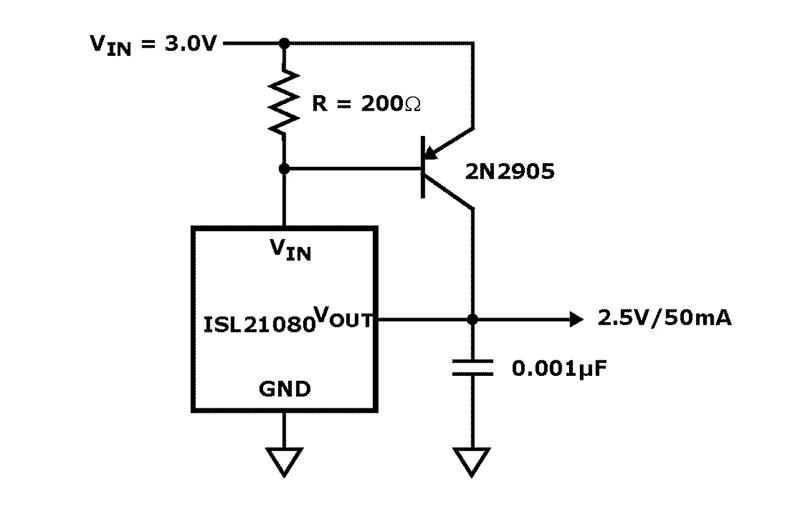
The ISL21080 analog voltage references feature low supply voltage operation at ultra-low 310nA typical, 1.5μA maximum operating current. Additionally, the ISL21080 family features ensured initial accuracy as low as ±0.2% and 50ppm/°C temperature coefficient. These references are ideal for general-purpose portable applications to extend battery life at a lower cost. The ISL21080 is provided in the industry standard 3 Ld SOT-23 pinout. The ISL21080 output voltages can be used as precision voltage sources for voltage monitors, control loops, standby voltages for low power states for DSP, FPGA, Datapath controllers, microcontrollers, and other core voltages: 0.9V, 1.024V, 1.25V, 1.5V, 2.048V, 2.5V, 3.0V, 3.3V, 4.096V, and 5.0V.
Special Note: Post-assembly X-ray inspection may lead to permanent changes in device output voltage and should be minimized or avoided. For further information, see “Applications Information” on page 15 of the datasheet and AN1533, “X-Ray Effects on Intersil FGA References”.
