Features
- PCIe Gen 1–7 compliant
- PCIe Gen 7 Common Clock jitter < 41fs RMS
- 276fs RMS typical phase jitter at 156.25MHz (12kHz to 20MHz)
- 2 programmable output pairs plus 1 LVCMOS REF output
- 1 integer, fractional or spread-spectrum output frequency per configuration
- 1MHz to 325MHz output frequency (LVDS or LP-HCSL)
- 1MHz to 200MHz output frequency (LVCMOS)
- 1.8V to 3.3V core VDD
- Individual 1.8V, 2.5V, or 3.3V VDDO for each programmable output pair
- Supports HCSL, LVDS, and LVCMOS I/O standards
- Supports AC-coupled LVPECL and CML logic – See AN-891
- 3mm × 3mm 16-LGA packages with 50MHz integrated crystal option
- Supported by Timing Commander™ software


Description
The 9FGV1006 is a member of Renesas' PhiClock™ programmable clock generator family. The 9FGV1006 provides two copies of a single integer, fractional or spread-spectrum output frequency and one copy of the crystal reference input. Two select pins allow for hardware selection of the desired configuration, or two I²C bits all easy software selection of the desired configuration. The user may configure any one of the four OTP configurations as the default when operating in I²C mode. Four unique I²C addresses are available, allowing easy I²C access to multiple components.
Try the Custom Part Configuration Utility.
Parameters
| Attributes | Value |
|---|---|
| Diff. Outputs | 2 |
| Diff. Output Signaling | LP-HCSL |
| Output Freq Range (MHz) | 100 - 100 |
| Accepts Spread Spec Input | Yes |
| Power Consumption Typ (mW) | 100 |
| Supply Voltage (V) | 1.8 - 1.8, 3.3 - 3.3 |
| Output Type | LP-HCSL |
| Xtal Freq (MHz) | 25 - 25, 50 - 50 |
| Package Area (mm²) | 25 |
| Battery Backup | No |
| Battery Seal | No |
| CPU Supervisory Function POR | No |
| Crystal Frequency Trimming | No |
| Frequency Out Pin | No |
| Inputs (#) | 1 |
| Input Freq (MHz) | 25 - 25, 50 - 50 |
| Function | Generator |
| Input Type | Crystal, LVCMOS |
| Output Banks (#) | 1 |
| Core Voltage (V) | 1.8, 3.3 |
| Output Voltage (V) | 1.8, 3.3 |
| Product Category | PCI Express Clocks |
Package Options
| Pkg. Type | Pkg. Dimensions (mm) | Lead Count (#) | Pitch (mm) |
|---|---|---|---|
| LGA | 3.0 x 3.0 x 1.1 | 16 | 0.5 |
Try the Custom Part Configuration Utility.
| Part Number | Status | Samples | Longevity | Stock | Package | Budgetary Price (USD) | Lead Count (#) | Carrier Type | Moisture Sensitivity Level (MSL) | Phase Jitter Typ RMS (ps) | Core Voltage (V) | Diff. Output Signaling | Input Freq (MHz) | Output Impedance | Output Type | Output Voltage (V) | Supply Voltage (V) | Xtal Freq (MHz) | Advanced Features | App Jitter Compliance | C-C Jitter Max P-P (ps) | Input Type | Outputs (#) | Output Freq Range (MHz) | Power Consumption Typ (mW) | Prog. Clock | Qty. per Reel (#) | Qty. per Carrier (#) | Xtal Inputs (#) | Pb (Lead) Free | Pb Free Category | Temp. Range (°C) | Country of Assembly | Country of Wafer Fabrication |
|---|---|---|---|---|---|---|---|---|---|---|---|---|---|---|---|---|---|---|---|---|---|---|---|---|---|---|---|---|---|---|---|---|---|---|
| 9FGV1006C001LTGI | Active | Available | 2040 Apr | Out of Stock | LGA | 16# | Tray | 3 | 0.283ps | 3.3V | LP-HCSL | 25 - 25 | 100 | LP-HCSL | 3.3V | 3.3 - 3.3 | 25 - 25 | Programmable Clock | PCIe Gen1, PCIe Gen2, PCIe Gen3, PCIe Gen4, PCIe Gen5, PCIe Gen6, PCIe Gen7 | 50ps | Crystal, LVCMOS | 2# | 100 - 100 | 100mW | Yes | 0 | 490# | 1# | Yes | e4 Au | -40 to 85°C | |||
| 9FGV1006C001LTGI8 | Active | N/A | 2040 Apr | Out of Stock | LGA | 16# | Reel | 3 | 0.283ps | 3.3V | LP-HCSL | 25 - 25 | 100 | LP-HCSL | 3.3V | 3.3 - 3.3 | 25 - 25 | Programmable Clock | PCIe Gen1, PCIe Gen2, PCIe Gen3, PCIe Gen4, PCIe Gen5, PCIe Gen6, PCIe Gen7 | 50ps | Crystal, LVCMOS | 2# | 100 - 100 | 100mW | Yes | 3000# | 0 | 1# | Yes | e4 Au | -40 to 85°C | |||
| 9FGV1006C002LTGI | Active | Available | 2040 Apr | Out of Stock | LGA | 16# | Tray | 3 | 0.29ps | 1.8V | LP-HCSL | 25 - 25 | 100 | LP-HCSL | 1.8V | 1.8 - 1.8 | 25 - 25 | Programmable Clock | PCIe Gen1, PCIe Gen2, PCIe Gen3, PCIe Gen4, PCIe Gen5, PCIe Gen6, PCIe Gen7 | 50ps | Crystal, LVCMOS | 2# | 100 - 100 | 100mW | Yes | 0 | 490# | 1# | Yes | e4 Au | -40 to 85°C | |||
| 9FGV1006C002LTGI8 | Active | N/A | 2040 Apr | Out of Stock | LGA | 16# | Reel | 3 | 0.29ps | 1.8V | LP-HCSL | 25 - 25 | 100 | LP-HCSL | 1.8V | 1.8 - 1.8 | 25 - 25 | Programmable Clock | PCIe Gen1, PCIe Gen2, PCIe Gen3, PCIe Gen4, PCIe Gen5, PCIe Gen6, PCIe Gen7 | 50ps | Crystal, LVCMOS | 2# | 100 - 100 | 100mW | Yes | 3000# | 0 | 1# | Yes | e4 Au | -40 to 85°C | |||
| 9FGV1006C015LTGI | Active | Available | 2040 Apr | Out of Stock | LGA | 16# | Tray | 3 | 0.283ps | 3.3V | LP-HCSL | 25 - 25 | 85 | LP-HCSL | 3.3V | 3.3 - 3.3 | 25 - 25 | Programmable Clock | PCIe Gen1, PCIe Gen2, PCIe Gen3, PCIe Gen4, PCIe Gen5, PCIe Gen6, PCIe Gen7 | 50ps | Crystal, LVCMOS | 2# | 100 - 100 | 100mW | Yes | 0 | 490# | 1# | Yes | e4 Au | -40 to 85°C | |||
| 9FGV1006C015LTGI8 | Active | N/A | 2040 Apr | Out of Stock | LGA | 16# | Reel | 3 | 0.283ps | 3.3V | LP-HCSL | 25 - 25 | 85 | LP-HCSL | 3.3V | 3.3 - 3.3 | 25 - 25 | Programmable Clock | PCIe Gen1, PCIe Gen2, PCIe Gen3, PCIe Gen4, PCIe Gen5, PCIe Gen6, PCIe Gen7 | 50ps | Crystal, LVCMOS | 2# | 100 - 100 | 100mW | Yes | 3000# | 0 | 1# | Yes | e4 Au | -40 to 85°C | |||
| 9FGV1006CQ505LTGI | Active | Available | 2040 Apr | Out of Stock | LGA | 16# | Tray | 3 | 0.26ps | 3.3V | LP-HCSL | 50 - 50 | 100 | LP-HCSL | 3.3V | 3.3 - 3.3 | 50 - 50 | Programmable Clock | PCIe Gen1, PCIe Gen2, PCIe Gen3, PCIe Gen4, PCIe Gen5, PCIe Gen6, PCIe Gen7 | 50ps | Crystal, LVCMOS | 2# | 100 - 100 | 100mW | Yes | 0 | 490# | 1# | Yes | e4 Au | -40 to 85°C | |||
| 9FGV1006CQ505LTGI8 | Active | N/A | 2040 Apr | Out of Stock | LGA | 16# | Reel | 3 | 0.26ps | 3.3V | LP-HCSL | 50 - 50 | 100 | LP-HCSL | 3.3V | 3.3 - 3.3 | 50 - 50 | Programmable Clock | PCIe Gen1, PCIe Gen2, PCIe Gen3, PCIe Gen4, PCIe Gen5, PCIe Gen6, PCIe Gen7 | 50ps | Crystal, LVCMOS | 2# | 100 - 100 | 100mW | Yes | 3000# | 0 | 1# | Yes | e4 Au | -40 to 85°C | |||
| 9FGV1006CQ506LTGI | Active | Available | 2040 Apr | Out of Stock | LGA | 16# | Tray | 3 | 0.258ps | 1.8V | LP-HCSL | 50 - 50 | 100 | LP-HCSL | 1.8V | 1.8 - 1.8 | 50 - 50 | Programmable Clock | PCIe Gen1, PCIe Gen2, PCIe Gen3, PCIe Gen4, PCIe Gen5, PCIe Gen6, PCIe Gen7 | 50ps | Crystal, LVCMOS | 2# | 100 - 100 | 100mW | Yes | 0 | 490# | 1# | Yes | e4 Au | -40 to 85°C | |||
| 9FGV1006CQ506LTGI8 | Active | N/A | 2040 Apr | Out of Stock | LGA | 16# | Reel | 3 | 0.258ps | 1.8V | LP-HCSL | 50 - 50 | 100 | LP-HCSL | 1.8V | 1.8 - 1.8 | 50 - 50 | Programmable Clock | PCIe Gen1, PCIe Gen2, PCIe Gen3, PCIe Gen4, PCIe Gen5, PCIe Gen6, PCIe Gen7 | 50ps | Crystal, LVCMOS | 2# | 100 - 100 | 100mW | Yes | 3000# | 0 | 1# | Yes | e4 Au | -40 to 85°C | |||
| 9FGV1006CQ515LTGI | Active | Available | 2040 Apr | Out of Stock | LGA | 1ku | $2.74 | 16# | Tray | 3 | 0.26ps | 3.3V | LP-HCSL | 50 - 50 | 85 | LP-HCSL | 3.3V | 3.3 - 3.3 | 50 - 50 | Programmable Clock | PCIe Gen1, PCIe Gen2, PCIe Gen3, PCIe Gen4, PCIe Gen5, PCIe Gen6, PCIe Gen7 | 50ps | Crystal, LVCMOS | 2# | 100 - 100 | 100mW | Yes | 0 | 490# | 1# | Yes | e4 Au | -40 to 85°C | TAIWAN | SINGAPORE |
| 9FGV1006CQ515LTGI8 | Active | N/A | 2040 Apr | Out of Stock | LGA | 1ku | $2.74 | 16# | Reel | 3 | 0.26ps | 3.3V | LP-HCSL | 50 - 50 | 85 | LP-HCSL | 3.3V | 3.3 - 3.3 | 50 - 50 | Programmable Clock | PCIe Gen1, PCIe Gen2, PCIe Gen3, PCIe Gen4, PCIe Gen5, PCIe Gen6, PCIe Gen7 | 50ps | Crystal, LVCMOS | 2# | 100 - 100 | 100mW | Yes | 3000# | 0 | 1# | Yes | e4 Au | -40 to 85°C | TAIWAN | SINGAPORE |
| 9FGV1006A000LTGI | Obsolete | N/A | Out of Stock | LGA | 16# | Tray | 3 | 0.31ps | 1.8V, 2.5V, 3.3V | LP-HCSL, LVDS | 8 - 50 | 85, 100 | LP-HCSL, LVCMOS, LVDS | 1.8V, 2.5V, 3.3V | 1.8 - 1.8, 2.5 - 2.5, 3.3 - 3.3 | 8 - 50 | Reference Output, Spread Spectrum, Programmable Clock | PCIe Gen1, PCIe Gen2, PCIe Gen3, PCIe Gen4, PCIe Gen5 | 50ps | Crystal, LVCMOS | 3# | 10 - 325 | 100mW | No | 0 | 490# | 1# | Yes | e4 Au | -40 to 85°C | ||||
| 9FGV1006A000LTGI8 | Obsolete | N/A | Out of Stock | LGA | 16# | Reel | 3 | 0.31ps | 1.8V, 2.5V, 3.3V | LP-HCSL, LVDS | 8 - 50 | 85, 100 | LP-HCSL, LVCMOS, LVDS | 1.8V, 2.5V, 3.3V | 1.8 - 1.8, 2.5 - 2.5, 3.3 - 3.3 | 8 - 50 | Reference Output, Spread Spectrum, Programmable Clock | PCIe Gen1, PCIe Gen2, PCIe Gen3, PCIe Gen4, PCIe Gen5 | 50ps | Crystal, LVCMOS | 3# | 10 - 325 | 100mW | No | 3000# | 0 | 1# | Yes | e4 Au | -40 to 85°C | ||||
| 9FGV1006A001LTGI | Obsolete | N/A | In Stock | LGA | 16# | Tray | 3 | 0.311ps | 3.3V | LP-HCSL | 25 - 25 | 100 | LP-HCSL | 3.3V | 1.8 - 1.8, 2.5 - 2.5, 3.3 - 3.3 | 25 - 25 | Programmable Clock | PCIe Gen1, PCIe Gen2, PCIe Gen3, PCIe Gen4, PCIe Gen5 | 25ps | Crystal, LVCMOS | 2# | 100 - 100 | 125mW | No | 0 | 490# | 1# | Yes | e4 Au | -40 to 85°C | ||||
| 9FGV1006A001LTGI8 | Obsolete | N/A | Out of Stock | LGA | 16# | Reel | 3 | 0.311ps | 3.3V | LP-HCSL | 25 - 25 | 100 | LP-HCSL | 3.3V | 1.8 - 1.8, 2.5 - 2.5, 3.3 - 3.3 | 25 - 25 | Programmable Clock | PCIe Gen1, PCIe Gen2, PCIe Gen3, PCIe Gen4, PCIe Gen5 | 25ps | Crystal, LVCMOS | 2# | 100 - 100 | 125mW | No | 3000# | 0 | 1# | Yes | e4 Au | -40 to 85°C | ||||
| 9FGV1006A002LTGI | Obsolete | N/A | In Stock | LGA | 16# | Tray | 3 | 0.32ps | 1.8V | LP-HCSL | 25 - 25 | 100 | LP-HCSL | 1.8V | 1.8 - 1.8, 2.5 - 2.5, 3.3 - 3.3 | 25 - 25 | Programmable Clock | PCIe Gen1, PCIe Gen2, PCIe Gen3, PCIe Gen4, PCIe Gen5 | 25ps | Crystal, LVCMOS | 2# | 100 - 100 | 100mW | No | 0 | 490# | 1# | Yes | e4 Au | -40 to 85°C | ||||
| 9FGV1006A002LTGI8 | Obsolete | N/A | Out of Stock | LGA | 16# | Reel | 3 | 0.32ps | 1.8V | LP-HCSL | 25 - 25 | 100 | LP-HCSL | 1.8V | 1.8 - 1.8, 2.5 - 2.5, 3.3 - 3.3 | 25 - 25 | Programmable Clock | PCIe Gen1, PCIe Gen2, PCIe Gen3, PCIe Gen4, PCIe Gen5 | 25ps | Crystal, LVCMOS | 2# | 100 - 100 | 100mW | No | 3000# | 0 | 1# | Yes | e4 Au | -40 to 85°C | ||||
| 9FGV1006A003LTGI | Obsolete | N/A | Out of Stock | LGA | 16# | Tray | 3 | 0.311ps | 3.3V | LVDS | 25 - 25 | 100 | LVDS | 3.3V | 1.8 - 1.8, 2.5 - 2.5, 3.3 - 3.3 | 25 - 25 | Programmable Clock | PCIe Gen1, PCIe Gen2, PCIe Gen3, PCIe Gen4, PCIe Gen5 | 25ps | Crystal, LVCMOS | 2# | 100 - 100 | 125mW | No | 0 | 490# | 1# | Yes | e4 Au | -40 to 85°C | ||||
| 9FGV1006A003LTGI8 | Obsolete | N/A | Out of Stock | LGA | 16# | Reel | 3 | 0.311ps | 3.3V | LVDS | 25 - 25 | 100 | LVDS | 3.3V | 1.8 - 1.8, 2.5 - 2.5, 3.3 - 3.3 | 25 - 25 | Programmable Clock | PCIe Gen1, PCIe Gen2, PCIe Gen3, PCIe Gen4, PCIe Gen5 | 25ps | Crystal, LVCMOS | 2# | 100 - 100 | 125mW | No | 3000# | 0 | 1# | Yes | e4 Au | -40 to 85°C | ||||
| 9FGV1006A004LTGI | Obsolete | N/A | Out of Stock | LGA | 16# | Tray | 3 | 0.32ps | 1.8V | LVDS | 25 - 25 | 100 | LVDS | 1.8V | 1.8 - 1.8, 2.5 - 2.5, 3.3 - 3.3 | 25 - 25 | Programmable Clock | PCIe Gen1, PCIe Gen2, PCIe Gen3, PCIe Gen4, PCIe Gen5 | 25ps | Crystal, LVCMOS | 2# | 100 - 100 | 100mW | No | 0 | 490# | 1# | Yes | e4 Au | -40 to 85°C | ||||
| 9FGV1006A004LTGI8 | Obsolete | N/A | Out of Stock | LGA | 16# | Reel | 3 | 0.32ps | 1.8V | LVDS | 25 - 25 | 100 | LVDS | 1.8V | 1.8 - 1.8, 2.5 - 2.5, 3.3 - 3.3 | 25 - 25 | Programmable Clock | PCIe Gen1, PCIe Gen2, PCIe Gen3, PCIe Gen4, PCIe Gen5 | 25ps | Crystal, LVCMOS | 2# | 100 - 100 | 100mW | No | 3000# | 0 | 1# | Yes | e4 Au | -40 to 85°C | ||||
| 9FGV1006B000LTGI | Obsolete | N/A | Out of Stock | LGA | 16# | Tray | 3 | 0.276ps | 1.8V, 2.5V, 3.3V | LP-HCSL, LVDS | 8 - 50 | 85, 100 | LP-HCSL, LVCMOS, LVDS | 1.8V, 2.5V, 3.3V | 1.8 - 1.8, 2.5 - 2.5, 3.3 - 3.3 | 8 - 50 | Reference Output, Spread Spectrum, Programmable Clock | PCIe Gen1, PCIe Gen2, PCIe Gen3, PCIe Gen4, PCIe Gen5 | 50ps | Crystal, LVCMOS | 3# | 10 - 325 | 100mW | No | 0 | 490# | 1# | Yes | e4 Au | -40 to 85°C | ||||
| 9FGV1006B000LTGI8 | Obsolete | N/A | Out of Stock | LGA | 16# | Reel | 3 | 0.276ps | 1.8V, 2.5V, 3.3V | LP-HCSL, LVDS | 8 - 50 | 85, 100 | LP-HCSL, LVCMOS, LVDS | 1.8V, 2.5V, 3.3V | 1.8 - 1.8, 2.5 - 2.5, 3.3 - 3.3 | 8 - 50 | Reference Output, Spread Spectrum, Programmable Clock | PCIe Gen1, PCIe Gen2, PCIe Gen3, PCIe Gen4, PCIe Gen5 | 50ps | Crystal, LVCMOS | 3# | 10 - 325 | 100mW | No | 3000# | 0 | 1# | Yes | e4 Au | -40 to 85°C | ||||
| 9FGV1006B001LTGI | Obsolete | N/A | In Stock | LGA | 16# | Tray | 3 | 0.276ps | 3.3V | LP-HCSL, LVDS | 8 - 50 | 100 | LP-HCSL, LVCMOS, LVDS | 1.8V, 2.5V, 3.3V | 1.8 - 1.8, 2.5 - 2.5, 3.3 - 3.3 | Reference Output, Spread Spectrum, Programmable Clock | PCIe Gen1, PCIe Gen2, PCIe Gen3, PCIe Gen4, PCIe Gen5 | 50ps | Crystal, LVCMOS | 3# | 10 - 325 | 100mW | No | 0 | 490# | 1# | Yes | e4 Au | -40 to 85°C | |||||
| 9FGV1006B001LTGI8 | Obsolete | N/A | Out of Stock | LGA | 16# | Reel | 3 | 0.276ps | 3.3V | LP-HCSL, LVDS | 8 - 50 | 100 | LP-HCSL, LVCMOS, LVDS | 1.8V, 2.5V, 3.3V | 1.8 - 1.8, 2.5 - 2.5, 3.3 - 3.3 | Reference Output, Spread Spectrum, Programmable Clock | PCIe Gen1, PCIe Gen2, PCIe Gen3, PCIe Gen4, PCIe Gen5 | 50ps | Crystal, LVCMOS | 3# | 10 - 325 | 100mW | No | 3000# | 0 | 1# | Yes | e4 Au | -40 to 85°C | |||||
| 9FGV1006B002LTGI | Obsolete | N/A | In Stock | LGA | 16# | Tray | 3 | 0.276ps | 1.8V | LP-HCSL, LVDS | 8 - 50 | 100 | LP-HCSL, LVCMOS, LVDS | 1.8V, 2.5V, 3.3V | 1.8 - 1.8, 2.5 - 2.5, 3.3 - 3.3 | Reference Output, Spread Spectrum, Programmable Clock | PCIe Gen1, PCIe Gen2, PCIe Gen3, PCIe Gen4, PCIe Gen5 | 50ps | Crystal, LVCMOS | 3# | 10 - 325 | 100mW | No | 0 | 490# | 1# | Yes | e4 Au | -40 to 85°C | |||||
| 9FGV1006B002LTGI8 | Obsolete | N/A | Out of Stock | LGA | 16# | Reel | 3 | 0.276ps | 1.8V | LP-HCSL, LVDS | 8 - 50 | 100 | LP-HCSL, LVCMOS, LVDS | 1.8V, 2.5V, 3.3V | 1.8 - 1.8, 2.5 - 2.5, 3.3 - 3.3 | Reference Output, Spread Spectrum, Programmable Clock | PCIe Gen1, PCIe Gen2, PCIe Gen3, PCIe Gen4, PCIe Gen5 | 50ps | Crystal, LVCMOS | 3# | 10 - 325 | 100mW | No | 3000# | 0 | 1# | Yes | e4 Au | -40 to 85°C | |||||
| 9FGV1006B015LTGI | Obsolete | N/A | Out of Stock | LGA | 16# | Tray | 3 | 0.276ps | 3.3V | LP-HCSL, LVDS | 8 - 50 | 85 | LP-HCSL, LVCMOS, LVDS | 1.8V, 2.5V, 3.3V | 1.8 - 1.8, 2.5 - 2.5, 3.3 - 3.3 | Reference Output, Spread Spectrum, Programmable Clock | PCIe Gen1, PCIe Gen2, PCIe Gen3, PCIe Gen4, PCIe Gen5 | 50ps | Crystal, LVCMOS | 3# | 10 - 325 | 100mW | No | 0 | 490# | 1# | Yes | e4 Au | -40 to 85°C | |||||
| 9FGV1006B015LTGI8 | Obsolete | N/A | Out of Stock | LGA | 16# | Reel | 3 | 0.276ps | 3.3V | LP-HCSL, LVDS | 8 - 50 | 85 | LP-HCSL, LVCMOS, LVDS | 1.8V, 2.5V, 3.3V | 1.8 - 1.8, 2.5 - 2.5, 3.3 - 3.3 | Reference Output, Spread Spectrum, Programmable Clock | PCIe Gen1, PCIe Gen2, PCIe Gen3, PCIe Gen4, PCIe Gen5 | 50ps | Crystal, LVCMOS | 3# | 10 - 325 | 100mW | No | 3000# | 0 | 1# | Yes | e4 Au | -40 to 85°C | |||||
| 9FGV1006BQ500LTGI | Obsolete | N/A | Out of Stock | LGA | 16# | Tray | 3 | 0.276ps | 1.8V, 2.5V, 3.3V | LP-HCSL, LVDS | 8 - 50 | 85, 100 | LP-HCSL, LVCMOS, LVDS | 1.8V, 2.5V, 3.3V | 1.8 - 1.8, 2.5 - 2.5, 3.3 - 3.3 | 8 - 50 | Reference Output, Spread Spectrum, Programmable Clock | PCIe Gen1, PCIe Gen2, PCIe Gen3, PCIe Gen4, PCIe Gen5 | 50ps | Crystal, LVCMOS | 3# | 10 - 325 | 100mW | No | 0 | 490# | 1# | Yes | e4 Au | -40 to 85°C | ||||
| 9FGV1006BQ500LTGI8 | Obsolete | N/A | Out of Stock | LGA | 16# | Reel | 3 | 0.276ps | 1.8V, 2.5V, 3.3V | LP-HCSL, LVDS | 8 - 50 | 85, 100 | LP-HCSL, LVCMOS, LVDS | 1.8V, 2.5V, 3.3V | 1.8 - 1.8, 2.5 - 2.5, 3.3 - 3.3 | 8 - 50 | Reference Output, Spread Spectrum, Programmable Clock | PCIe Gen1, PCIe Gen2, PCIe Gen3, PCIe Gen4, PCIe Gen5 | 50ps | Crystal, LVCMOS | 3# | 10 - 325 | 100mW | No | 3000# | 0 | 1# | Yes | e4 Au | -40 to 85°C | ||||
| 9FGV1006BQ505LTGI | Obsolete | N/A | Out of Stock | LGA | 16# | Tray | 3 | 0.276ps | 3.3V | LP-HCSL, LVDS | 8 - 50 | 100 | LP-HCSL, LVCMOS, LVDS | 1.8V, 2.5V, 3.3V | 1.8 - 1.8, 2.5 - 2.5, 3.3 - 3.3 | Reference Output, Spread Spectrum, Programmable Clock | PCIe Gen1, PCIe Gen2, PCIe Gen3, PCIe Gen4, PCIe Gen5 | 50ps | Crystal, LVCMOS | 3# | 10 - 325 | 100mW | No | 0 | 490# | 1# | Yes | e4 Au | -40 to 85°C | |||||
| 9FGV1006BQ505LTGI8 | Obsolete | N/A | Out of Stock | LGA | 16# | Reel | 3 | 0.276ps | 3.3V | LP-HCSL, LVDS | 8 - 50 | 100 | LP-HCSL, LVCMOS, LVDS | 1.8V, 2.5V, 3.3V | 1.8 - 1.8, 2.5 - 2.5, 3.3 - 3.3 | Reference Output, Spread Spectrum, Programmable Clock | PCIe Gen1, PCIe Gen2, PCIe Gen3, PCIe Gen4, PCIe Gen5 | 50ps | Crystal, LVCMOS | 3# | 10 - 325 | 100mW | No | 3000# | 0 | 1# | Yes | e4 Au | -40 to 85°C | |||||
| 9FGV1006BQ506LTGI | Obsolete | N/A | Out of Stock | LGA | 16# | Tray | 3 | 0.276ps | 1.8V | LP-HCSL, LVDS | 8 - 50 | 100 | LP-HCSL, LVCMOS, LVDS | 1.8V, 2.5V, 3.3V | 1.8 - 1.8, 2.5 - 2.5, 3.3 - 3.3 | Reference Output, Spread Spectrum, Programmable Clock | PCIe Gen1, PCIe Gen2, PCIe Gen3, PCIe Gen4, PCIe Gen5 | 50ps | Crystal, LVCMOS | 3# | 10 - 325 | 100mW | No | 0 | 490# | 1# | Yes | e4 Au | -40 to 85°C | |||||
| 9FGV1006BQ506LTGI8 | Obsolete | N/A | Out of Stock | LGA | 16# | Reel | 3 | 0.276ps | 1.8V | LP-HCSL, LVDS | 8 - 50 | 100 | LP-HCSL, LVCMOS, LVDS | 1.8V, 2.5V, 3.3V | 1.8 - 1.8, 2.5 - 2.5, 3.3 - 3.3 | Reference Output, Spread Spectrum, Programmable Clock | PCIe Gen1, PCIe Gen2, PCIe Gen3, PCIe Gen4, PCIe Gen5 | 50ps | Crystal, LVCMOS | 3# | 10 - 325 | 100mW | No | 3000# | 0 | 1# | Yes | e4 Au | -40 to 85°C | |||||
| 9FGV1006BQ515LTGI | Obsolete | N/A | Out of Stock | LGA | 16# | Tray | 3 | 0.276ps | 3.3V | LP-HCSL, LVDS | 8 - 50 | 85 | LP-HCSL, LVCMOS, LVDS | 1.8V, 2.5V, 3.3V | 1.8 - 1.8, 2.5 - 2.5, 3.3 - 3.3 | Reference Output, Spread Spectrum, Programmable Clock | PCIe Gen1, PCIe Gen2, PCIe Gen3, PCIe Gen4, PCIe Gen5 | 50ps | Crystal, LVCMOS | 3# | 10 - 325 | 100mW | No | 0 | 490# | 1# | Yes | e4 Au | -40 to 85°C | |||||
| 9FGV1006BQ515LTGI8 | Obsolete | N/A | Out of Stock | LGA | 16# | Reel | 3 | 0.276ps | 3.3V | LP-HCSL, LVDS | 8 - 50 | 85 | LP-HCSL, LVCMOS, LVDS | 1.8V, 2.5V, 3.3V | 1.8 - 1.8, 2.5 - 2.5, 3.3 - 3.3 | Reference Output, Spread Spectrum, Programmable Clock | PCIe Gen1, PCIe Gen2, PCIe Gen3, PCIe Gen4, PCIe Gen5 | 50ps | Crystal, LVCMOS | 3# | 10 - 325 | 100mW | No | 3000# | 0 | 1# | Yes | e4 Au | -40 to 85°C | |||||
| 9FGV1006Q500LTGI | Obsolete | N/A | Out of Stock | LGA | 16# | Tray | 3 | 0.31ps | 1.8V, 2.5V, 3.3V | LP-HCSL, LVDS | 8 - 50 | 85, 100 | LP-HCSL, LVCMOS, LVDS | 1.8V, 2.5V, 3.3V | 1.8 - 1.8, 2.5 - 2.5, 3.3 - 3.3 | 50 - 50 | Reference Output, Spread Spectrum, Programmable Clock | PCIe Gen1, PCIe Gen2, PCIe Gen3, PCIe Gen4, PCIe Gen5 | 50ps | Crystal, LVCMOS | 3# | 10 - 325 | 100mW | No | 0 | 490# | 1# | Yes | e4 Au | -40 to 85°C | ||||
| 9FGV1006Q500LTGI8 | Obsolete | N/A | Out of Stock | LGA | 16# | Reel | 3 | 0.31ps | 1.8V, 2.5V, 3.3V | LP-HCSL, LVDS | 8 - 50 | 85, 100 | LP-HCSL, LVCMOS, LVDS | 1.8V, 2.5V, 3.3V | 1.8 - 1.8, 2.5 - 2.5, 3.3 - 3.3 | 50 - 50 | Reference Output, Spread Spectrum, Programmable Clock | PCIe Gen1, PCIe Gen2, PCIe Gen3, PCIe Gen4, PCIe Gen5 | 50ps | Crystal, LVCMOS | 3# | 10 - 325 | 100mW | No | 3000# | 0 | 1# | Yes | e4 Au | -40 to 85°C | ||||
| 9FGV1006Q505LTGI | Obsolete | N/A | Out of Stock | LGA | 16# | Tray | 3 | 0.296ps | 3.3V | LP-HCSL | 50 - 50 | 100 | LP-HCSL | 3.3V | 1.8 - 1.8, 2.5 - 2.5, 3.3 - 3.3 | 50 - 50 | Programmable Clock | PCIe Gen1, PCIe Gen2, PCIe Gen3, PCIe Gen4, PCIe Gen5 | 50ps | Crystal (integrated) | 2# | 100 - 100 | 125mW | No | 0 | 490# | 0 | Yes | e4 Au | -40 to 85°C | ||||
| 9FGV1006Q505LTGI8 | Obsolete | N/A | Out of Stock | LGA | 16# | Reel | 3 | 0.296ps | 3.3V | LP-HCSL | 50 - 50 | 100 | LP-HCSL | 3.3V | 1.8 - 1.8, 2.5 - 2.5, 3.3 - 3.3 | 50 - 50 | Programmable Clock | PCIe Gen1, PCIe Gen2, PCIe Gen3, PCIe Gen4, PCIe Gen5 | 50ps | Crystal (integrated) | 2# | 100 - 100 | 125mW | No | 3000# | 0 | 0 | Yes | e4 Au | -40 to 85°C | ||||
| 9FGV1006Q506LTGI | NRND | Available | Out of Stock | LGA | 16# | Tray | 3 | 0.305ps | 1.8V | LP-HCSL | 50 - 50 | 100 | LP-HCSL | 1.8V | 1.8 - 1.8, 2.5 - 2.5, 3.3 - 3.3 | 50 - 50 | Programmable Clock | PCIe Gen1, PCIe Gen2, PCIe Gen3, PCIe Gen4, PCIe Gen5 | 50ps | Crystal (integrated) | 2# | 100 - 100 | 100mW | No | 0 | 490# | 0 | Yes | e4 Au | -40 to 85°C | ||||
| 9FGV1006Q506LTGI8 | NRND | N/A | Out of Stock | LGA | 16# | Reel | 3 | 0.305ps | 1.8V | LP-HCSL | 50 - 50 | 100 | LP-HCSL | 1.8V | 1.8 - 1.8, 2.5 - 2.5, 3.3 - 3.3 | 50 - 50 | Programmable Clock | PCIe Gen1, PCIe Gen2, PCIe Gen3, PCIe Gen4, PCIe Gen5 | 50ps | Crystal (integrated) | 2# | 100 - 100 | 100mW | No | 3000# | 0 | 0 | Yes | e4 Au | -40 to 85°C | ||||
| 9FGV1006Q507LTGI | Obsolete | N/A | Out of Stock | LGA | 16# | Tray | 3 | 0.296ps | 3.3V | LVDS | 50 - 50 | 100 | LVDS | 3.3V | 1.8 - 1.8, 2.5 - 2.5, 3.3 - 3.3 | 50 - 50 | Programmable Clock | PCIe Gen1, PCIe Gen2, PCIe Gen3, PCIe Gen4, PCIe Gen5 | 50ps | Crystal (integrated) | 2# | 100 - 100 | 125mW | No | 0 | 490# | 0 | Yes | e4 Au | -40 to 85°C | ||||
| 9FGV1006Q507LTGI8 | Obsolete | N/A | Out of Stock | LGA | 16# | Reel | 3 | 0.296ps | 3.3V | LVDS | 50 - 50 | 100 | LVDS | 3.3V | 1.8 - 1.8, 2.5 - 2.5, 3.3 - 3.3 | 50 - 50 | Programmable Clock | PCIe Gen1, PCIe Gen2, PCIe Gen3, PCIe Gen4, PCIe Gen5 | 50ps | Crystal (integrated) | 2# | 100 - 100 | 125mW | No | 3000# | 0 | 0 | Yes | e4 Au | -40 to 85°C | ||||
| 9FGV1006Q508LTGI | Obsolete | N/A | Out of Stock | LGA | 16# | Tray | 3 | 0.305ps | 1.8V | LVDS | 50 - 50 | 100 | LVDS | 1.8V | 1.8 - 1.8, 2.5 - 2.5, 3.3 - 3.3 | 50 - 50 | Programmable Clock | PCIe Gen1, PCIe Gen2, PCIe Gen3, PCIe Gen4, PCIe Gen5 | 50ps | Crystal (integrated) | 2# | 100 - 100 | 100mW | No | 0 | 490# | 0 | Yes | e4 Au | -40 to 85°C | ||||
| 9FGV1006Q508LTGI8 | Obsolete | N/A | Out of Stock | LGA | 16# | Reel | 3 | 0.305ps | 1.8V | LVDS | 50 - 50 | 100 | LVDS | 1.8V | 1.8 - 1.8, 2.5 - 2.5, 3.3 - 3.3 | 50 - 50 | Programmable Clock | PCIe Gen1, PCIe Gen2, PCIe Gen3, PCIe Gen4, PCIe Gen5 | 50ps | Crystal (integrated) | 2# | 100 - 100 | 100mW | No | 3000# | 0 | 0 | Yes | e4 Au | -40 to 85°C |
Filters
Applied Filters
- Application NotePDF 1.53 MB R31AN0034EU0102 Rev.1.02 Oct 21, 2025AI-generated Summary: PLL loop filter design involves selecting component values to ensure stable operation and optimized phase noise. The loop bandwidth depends on parameters like charge pump current, VCO gain, and feedback divider. Second and third order passive loop filters are common, with specific calculations for cutoff, zero, and pole frequencies guiding component selection. Proper tuning of loop bandwidth enhances PLL stability and phase noise performance, demonstrated through lab experiments and calculation examples.
- Application NotePDF 431 KB 7WDXRDKU4E7E-5-59216 Dec 06, 2023
- Application NotePDF 256 KB Jul 05, 2021AI-generated Summary: The document explains methods to generate a 1.2V LVCMOS signal from a 1.8V LVCMOS output by attenuating the amplitude without lowering the driver voltage. It details typical LVCMOS driver and receiver configurations, impedance matching using source termination, and the use of a parallel resistor at the receiver input to reduce signal amplitude. Simulation and measurement results demonstrate that adding a parallel resistor effectively lowers the voltage to 1.2V while maintaining signal integrity and minimal impact on jitter and frequency. This approach supports flexible amplitude adjustment for various low-voltage LVCMOS requirements in clock signal applications.
Recommended Documents (1)
Datasheets (7)
- Manual - SoftwarePDF 323 KB 7WDXRDKU4E7E-5-62422 Feb 23, 2018
- Manual - SoftwarePDF 401 KB 7WDXRDKU4E7E-5-62508 Nov 27, 2017
Manuals & Guides (3)
- Application NotePDF 1.53 MB R31AN0034EU0102 Rev.1.02 Oct 21, 2025AI-generated Summary: PLL loop filter design involves selecting component values to ensure stable operation and optimized phase noise. The loop bandwidth depends on parameters like charge pump current, VCO gain, and feedback divider. Second and third order passive loop filters are common, with specific calculations for cutoff, zero, and pole frequencies guiding component selection. Proper tuning of loop bandwidth enhances PLL stability and phase noise performance, demonstrated through lab experiments and calculation examples.
- Application NotePDF 431 KB 7WDXRDKU4E7E-5-59216 Dec 06, 2023
- Application NotePDF 1.99 MB 7WDXRDKU4E7E-5-57242 Mar 01, 2022
- Application NotePDF 256 KB Jul 05, 2021AI-generated Summary: The document explains methods to generate a 1.2V LVCMOS signal from a 1.8V LVCMOS output by attenuating the amplitude without lowering the driver voltage. It details typical LVCMOS driver and receiver configurations, impedance matching using source termination, and the use of a parallel resistor at the receiver input to reduce signal amplitude. Simulation and measurement results demonstrate that adding a parallel resistor effectively lowers the voltage to 1.2V while maintaining signal integrity and minimal impact on jitter and frequency. This approach supports flexible amplitude adjustment for various low-voltage LVCMOS requirements in clock signal applications.View More (21)
Application Notes & White Papers (21)
- Product Change NoticePDF 761 KB 7WDXRDKU4E7E-5-63278 Sep 25, 2018
Product Notices (PCN, EOL, etc) (3)
No Results Found.
Make sure all keywords are spelled correctly.
Try fewer, different, or more general terms to vary your search.
If you have filters applied, consider deselecting some to broaden your results.
- Search our extensive knowledgebase, designed to help customers with their FAQs.
- Get help from our expert Renesas technical staff and community on our support forums.
Schematics & Design Files (1)
No Results Found.
Make sure all keywords are spelled correctly.
Try fewer, different, or more general terms to vary your search.
If you have filters applied, consider deselecting some to broaden your results.
- Search our extensive knowledgebase, designed to help customers with their FAQs.
- Get help from our expert Renesas technical staff and community on our support forums.
Marketing Collateral (1)
Other (1)
No Results Found.
Make sure all keywords are spelled correctly.
Try fewer, different, or more general terms to vary your search.
If you have filters applied, consider deselecting some to broaden your results.
- Search our extensive knowledgebase, designed to help customers with their FAQs.
- Get help from our expert Renesas technical staff and community on our support forums.
Renesas Boards & Kits
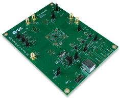
Evaluation Kit for 9FGV1006 Programmable PhiClock™ Generator
This is the evaluation board for the 9FGV1006 programmable PhiClockTM generator. It provides a convenient way of configuring and programming the blank parts for the 9FGV1006 device. With the onboard USB interface, the Renesas Timing CommanderTM graphical user interface (GUI) can communicate with... Read More
Evaluation Kit for 9FGV1006 Programmable PhiClock™ Generator with Internal 50MHz Crystal
This is the evaluation board for the 9FGV1006Q5 programmable PhiClockTM generator with an internal 50MHz crystal. It provides a convenient way of configuring and programming the blank parts for the 9FGV1006Q5 device. With the onboard USB interface, the Renesas Timing CommanderTM graphical user... Read More
