| Lead Count (#) | 56 |
| Pkg. Code | NLG56 |
| Pitch (mm) | 0.5 |
| Pkg. Type | VFQFPN |
| Pkg. Dimensions (mm) | 8.0 x 8.0 x 0.85 |
| Moisture Sensitivity Level (MSL) | 3 |
| Pb (Lead) Free | Yes |
| ECCN (US) | NLR |
| HTS (US) | 8542390001 |
| Lead Count (#) | 56 |
| Carrier Type | Reel |
| Moisture Sensitivity Level (MSL) | 3 |
| Qty. per Reel (#) | 3000 |
| Qty. per Carrier (#) | 0 |
| Pb (Lead) Free | Yes |
| Pb Free Category | e3 Sn |
| Temp. Range | -40 to +85°C |
| Country of Assembly | Taiwan |
| Country of Wafer Fabrication | Singapore |
| Advanced Features | Programmable Hitless Reference Switching, Fractional-N PLL, External Feedback |
| Application | Jitter Attenuator, Port Synchronizer |
| Channels (#) | 2 |
| Core Voltage (V) | 2.5, 3.3 |
| Diff. Inputs | 2 |
| Diff. Outputs | 8 |
| Family Name | UFT (Gen 3) |
| Feedback Input | Yes |
| Fractional Output Dividers (#) | 2 |
| Input Freq (MHz) | 0.008 - 875 |
| Input Freq Range Type | TDM, DS1, E1, SONET/SDH, Ethernet, OTN |
| Input Type | LVCMOS, LVTTL, HCSL, LVHSTL, LVDS, LVPECL |
| Inputs (#) | 2 |
| Length (mm) | 8 |
| Loop Bandwidth Range (Hz) | 0.5 - 360 |
| MOQ | 3000 |
| Output Banks (#) | 4 |
| Output Freq Range (MHz) | 0.008 - 1000 |
| Output Freq Range Type | TDM, DS1, E1, DS2, E3, DS3, 100BASE-T, STM-1/OC-3, STM-4/OC-12, 1000BASE-T/X, STM-16/OC-48, OTU-1, STM-64/OC-192/10GBASE-W, 10GBASE-R, OTU-2, XGMII/XAUI |
| Output Signaling | LVCMOS, LVDS, LVPECL, HCSL |
| Output Skew (ps) | 45 |
| Output Type | LVCMOS, LVDS, LVPECL, HCSL |
| Output Voltage (V) | 2.5, 3.3 |
| Outputs (#) | 8 |
| Package Area (mm²) | 64.0 |
| Phase Jitter Typ RMS (fs) | 280.000 |
| Phase Jitter Typ RMS (ps) | 0.280 |
| Pitch (mm) | 0.5 |
| Pkg. Dimensions (mm) | 8.0 x 8.0 x 0.85 |
| Pkg. Type | VFQFPN |
| Product Category | FemtoClock NG |
| Prog. Clock | Yes |
| Prog. Interface | I2C |
| Reel Size (in) | 13 |
| Reference Output | Yes |
| Requires Terms and Conditions | Does not require acceptance of Terms and Conditions |
| Spread Spectrum | No |
| Tape & Reel | Yes |
| Thickness (mm) | 0.85 |
| VCO Max Freq (MHz) | 4000 |
| VCO Min Freq (MHz) | 3000 |
| Width (mm) | 8 |
| Xtal Freq (KHz) | 10000 - 40000 |
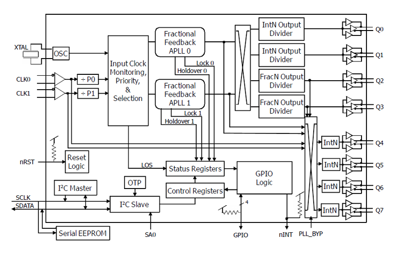
The 8T49N287 has two fractional feedback PLL’s that can be used as a frequency translators with jitter attenuation or a frequency synthesizers. It is equipped with six integer and two fractional output dividers, allowing the generation of up to eight different output frequencies, ranging from 8 kHz to 1 GHz. Output frequencies can be completely independent of the input frequencies, and up to four of these frequencies can be completely independent of each other. The eight outputs may select among LVPECL, LVDS, HCSL or LVCMOS output levels.
The 8T49N287 is ideal for use in a wide range of equipment, including 10G/40G/100G SONET/SDH and Ethernet network line cards, wireless base station baseband units, broadcast video, carrier Ethernet switches, OTN, or on test and measurement applications. The 8T49N287 can be used in GbE/10GbE/100GbE Synchronous Ethernet line card applications in order to preserve the G.8262 compliance from the Synchronous Equipment Timing Source (SETS) on the timing card.
Renesas’ third generation Universal Frequency Translator family also includes the 8T49N285 (2-in / 1-PLL / 8-out), 8T49N286 (4-in / 2-PLL / 8-out), and the 8T49N242 (2-in / 1-PLL / 4-out). These devices are complemented by the 82P33714 and 82P33731 synchronous equipment timing source (SETS) for Synchronous Ethernet (SyncE) and 10G-40G SyncE, respectively.
To see other devices in this product family, visit the Universal Frequency Translators page.