Warning message
Please log in or register to access this secure document.
Features
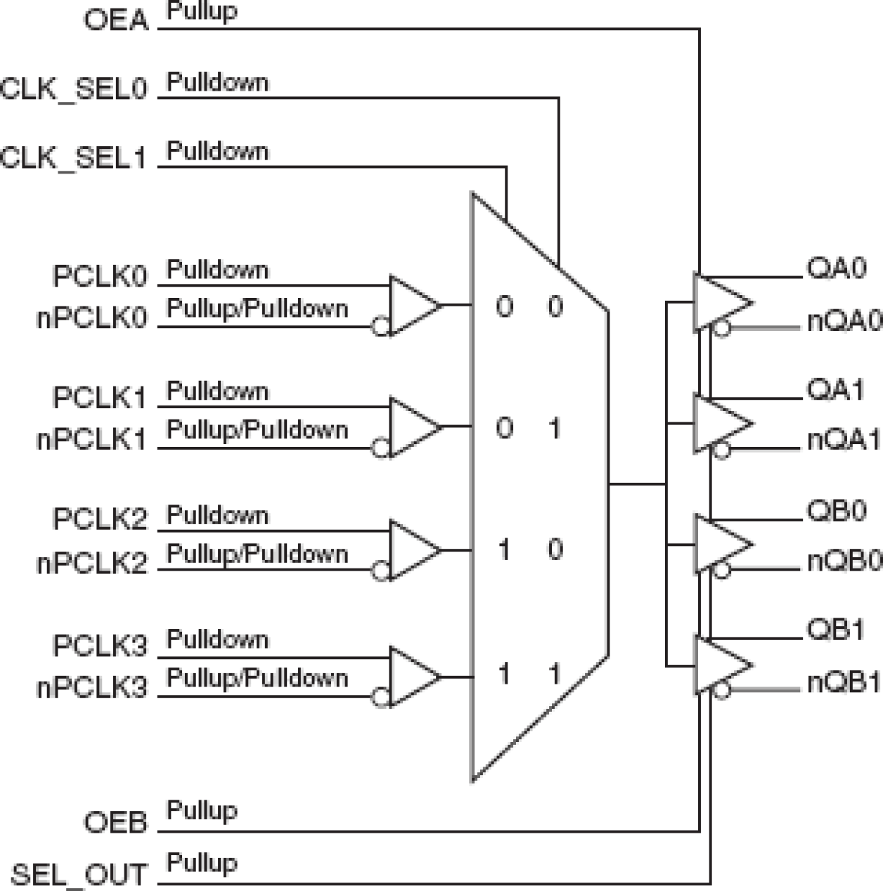
- High speed 4:1 differential multiplexer with a 1:4 fanout buffer
- Four programmable differential LVPECL or LVDS output pairs
- Four selectable differential PCLKx, nPCLKx input pairs
- PCLKx, nPCLKx pairs can accept the following differential input levels: LVPECL, LVDS, CML
- Maximum output frequency: 3GHz
- Translates any single ended input signal to LVPECL levels with resistor bias on nPCLKx inputs
- Part-to-part skew: 100ps (maximum)
- Propagation delay: 555ps (typical) @ 3.3V
- Additive phase jitter, RMS: 0.22ps (typical) @ 3.3V
- Full 3.3V or 2.5V supply modes
- -40°C to 85°C ambient operating temperature
- Available in lead-free (RoHS 6) package
Description
The 859S0424I is a 4:4 Differential-to-LVPECL/ LVDS Clock Multiplexer which can operate up to 3GHz. The outputs for this device can either be programmed to give LVPECL or LVDS levels. The 859S0424I has four selectable differential PCLKx, nPCLKx clock inputs. The PCLKx, nPCLKx input pairs can accept LVPECL, LVDS or CML levels. The fully differential architecture and low propagation delay make it ideal for use in clock distribution circuits.
Applied Filters:


