Overview
Description
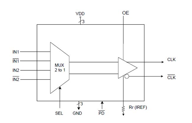
The 6V31023 is a 2:1 differential clock mux for PCI Express applications. It has very low additive jitter making it suitable for use in PCIe Gen2 and Gen3 systems. The 6V31023 selects between 1 of 2 differential HCSL inputs to drive a single differential HCSL output pair. The output can also be terminated to LVDS.
Features
- Low additive jitter suitable for use in PCIe Gen2 and Gen3 systems
- 16-pin TSSOP package for small board footprint
- Outputs can be terminated to LVDS to drive a wider variety of devices
- OE control pin offers greater system power management
- Industrial temperature range supports demanding embedded applications
- Additive cycle-to-cycle jitter <5 ps
- Additive phase jitter (PCIe Gen3) <0.2ps
- Operating frequency up to 200MHz
Comparison
Applications
Design & Development
Models
ECAD Models
Schematic symbols, PCB footprints, and 3D CAD models from SamacSys can be found by clicking on the CAD Model links in the Product Options table. If a symbol or model isn't available, it can be requested directly from SamacSys.

Product Options
Applied Filters:
Videos & Training
PCIe Clocking Architectures (Common and Separate)
This is the first video in our PCIe series. In this video, we define PCIe architectures, focusing on common and separate clock architectures. Watch the rest of the video series below where Ron will cover the impact of different timing architectures.
Watch the Video Series Below

Video List