特長
- Dual 1:2 low skew, low additive jitter LVDS fanout buffers
- Matched AC characteristics across both channels
- High isolation between channels
- Low power consumption
- Both differential CLKA, nCLKA and CLKB, nCLKB inputs accept LVDS, LVPECL and single-ended LVCMOS levels
- Maximum input clock frequency: 2.0GHz
- Output amplitudes: 350mV, 500mV (selectable)
- Output bank skew: 5ps typical
- Output skew: 30ps typical
- Low additive phase jitter, RMS: 40fs typical (fREF = 156.25MHz, 12kHz to 20MHz)
- Full 1.8V / 2.5V supply voltage mode
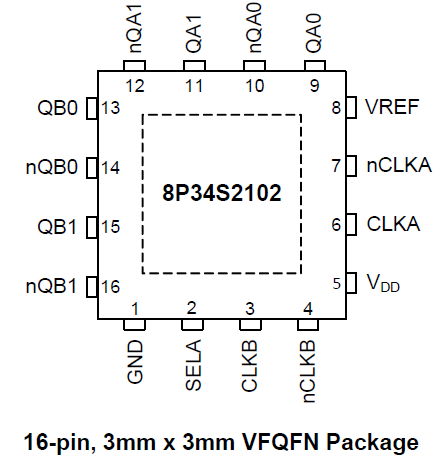
- Lead-free (RoHS 6), 16-lead VFQFN packaging
- -40°C to 85°C (Tc ≤ 105°C) operating temperature range
説明
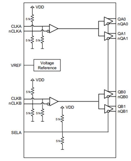
The 8P34S2102 is a high-performance, low-power, differential dual 1:2 LVDS output, 1.8V/2.5V fanout buffer. The device supports fail-safe operation and is designed for the fanout of high-frequency, very low additive phase-noise clock and data signals. Two independent buffer channels are available. Each channel has two low-skew outputs. High isolation between channels minimizes noise coupling. AC characteristics such as propagation delay are matched between channels. Guaranteed output-to-output and part-to-part skew characteristics make the 8P34S2102 ideal for those clock distribution applications demanding well-defined performance and repeatability. The device is characterized to operate from a 1.8V or a 2.5V power supply. The integrated bias voltage references enable easy interfacing of AC-coupled signals to the device inputs.
パラメータ
| 属性 | 値 |
|---|---|
| Outputs (#) | 4 |
| Inputs (#) | 2 |
| Channels (#) | 2 |
| Input Freq (MHz) | - |
| Output Freq Range (MHz) | - |
| Output Skew (ps) | 30 |
| Adjustable Phase | No |
| Noise Floor (dBc/Hz) | -160 |
| Additive Phase Jitter Typ RMS (fs) | 45 |
| Output Type | LVDS |
| Supply Voltage (V) | - |
| Advanced Features | Dual Buffer, Output Amplitude Control |
| 105°C Max. Case Temp. | 1 |
パッケージオプション
| Pkg. Type | Pkg. Dimensions (mm) | Lead Count (#) | Pitch (mm) |
|---|---|---|---|
| VFQFPN | 3.0 x 3.0 x 1.0 | 16 | 0.5 |