Features
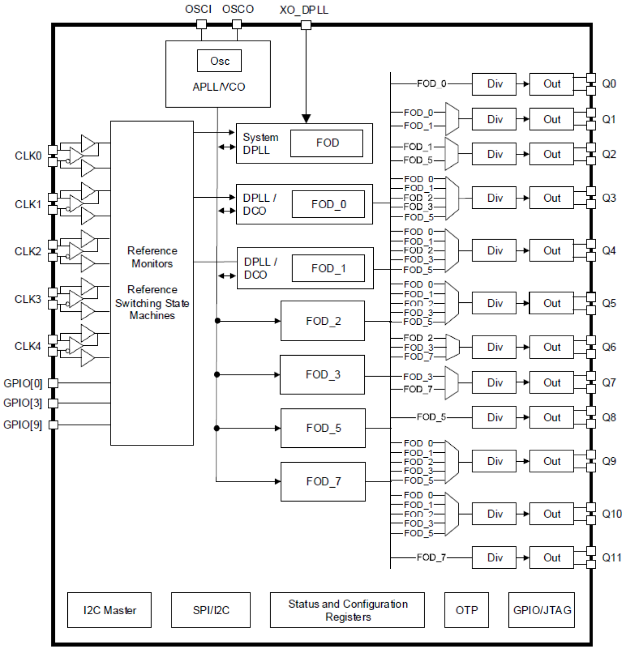
- Two timing channels and six independent frequency domains
- Output jitter below 100fs RMS
- Digital PLLs (DPLLs) lock to any frequency from 0.5kHz to 1GHz
- DPLLs/Digitally Controlled Oscillators (DCOs) generate any frequency from 0.5Hz to 1GHz
- DCO outputs can be aligned in phase and frequency with the outputs of any DPLL or DCO
- Can be used as a jitter attenuator, clock generator, or synchronizer
- Reference monitors qualify/disqualify references depending on LOS, activity, frequency monitoring, and/or LOS input pins
- Automatic reference selection state machines select the active reference for each DPLL based on the reference monitors, priority tables, revertive/non-revertive, and other programmable settings
- Device requires a crystal oscillator or fundamental-mode crystal: 25MHz to 54MHz
- The device can configure itself automatically after reset via:
- Internal customer-programmable one-time programmable (OTP) memory
- Standard external I²C EPROM via separate I²C Master Port
Description
The RC32112A regenerates and distributes ultra-low jitter clock outputs and features up to six independent frequency domains that can be either locked to the external reference clock or locked to a free-run crystal or oscillator. Digital PLLs (DPLLs) support hitless reference switching between references from redundant timing sources. The device supports multiple independent timing channels for IEEE 1588 clock synthesis, SyncE clock generation, jitter attenuation, and radio clock generation including SYSREF generation for converters. Input-to-input, input-to-output, and output-to-output phase skew can all be precisely managed. The device outputs ultra-low jitter clocks that can directly synchronize SerDes running at up to 56Gbps; as well as CPRI/OBSAI, SONET/SDH ADC/DAC. The device is ideal for use in 100G/200G/400G/800G telecom switch line cards, fabric cards, and wireless small cell applications.
Parameters
| Attributes | Value |
|---|---|
| Product Category | Jitter Attenuators |
Applied Filters:


