Features
- Fifteen single ended LVCMOS outputs, 7? typical output impedance
- Selectable LVCMOS or LVPECL clock inputs
- CLK0 and CLK1 can accept the following input levels: LVCMOS and LVTTL
- PCLK, nPCLK supports the following input types: LVPECL, CML, SSTL
- Maximum output frequency: 160MHz
- Output skew: 350ps (maximum)
- Part-to-part skew: 2.75ns (maximum)
- 3.3V supply voltage
- -40°C to 85°C ambient operating temperature
- Available in lead-free RoHS compliant packages
Description
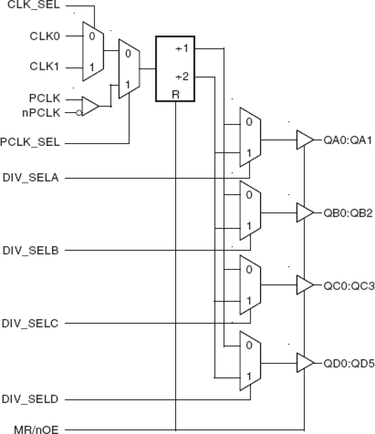
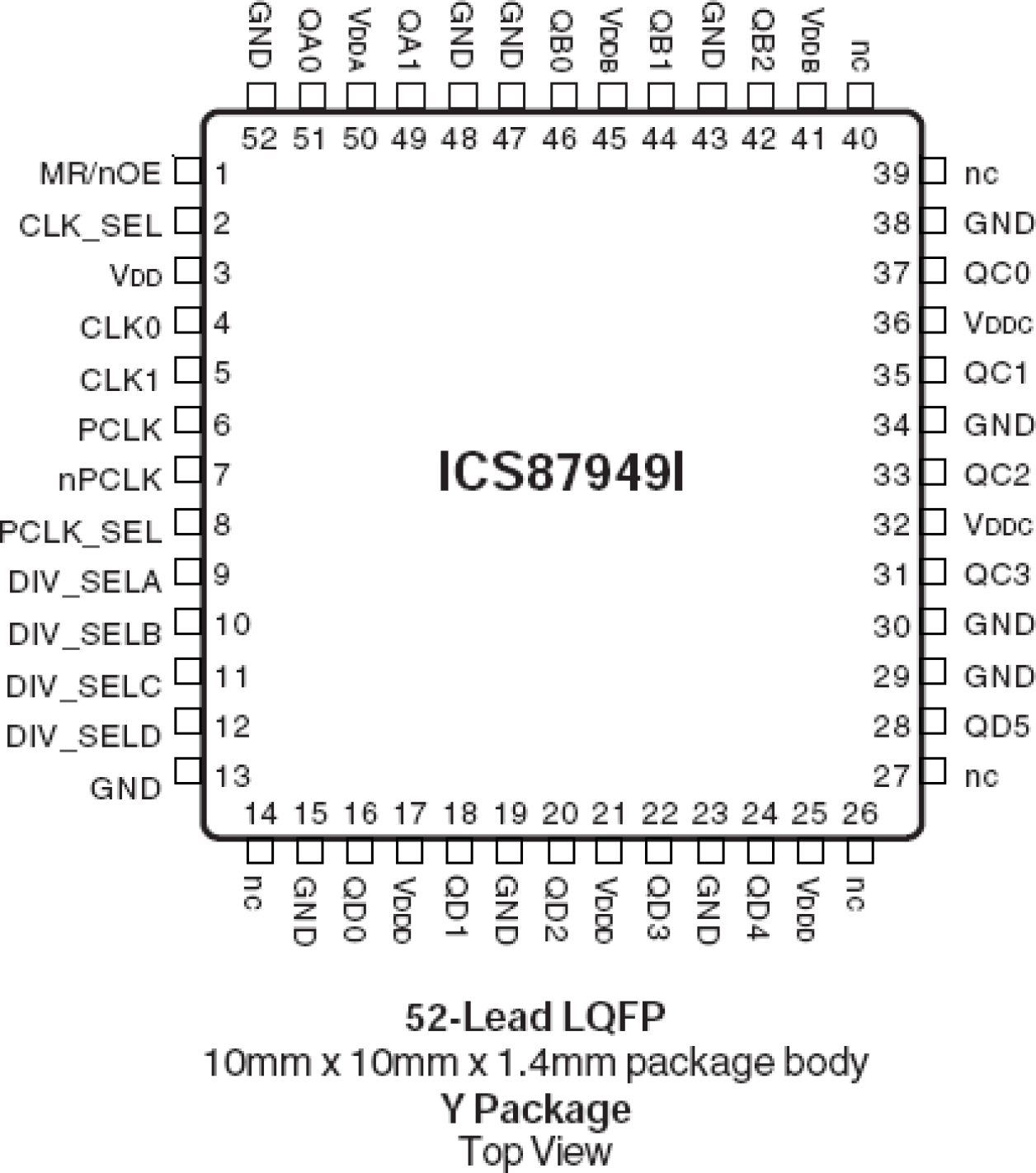
The 87949I is a low skew, ÷1, ÷2 Clock Generator. The 87949I has selectable single ended clock or LVPECL clock inputs. The single ended clock input accepts LVCMOS or LVTTL input levels. The PCLK, nPCLK pair can accept LVPECL, CML, or SSTL input levels. The low impedance LVCMOS outputs are designed to drive 50? series or parallel terminated transmission lines. The effective fanout can be increased from 15 to 30 by utilizing the ability of the outputs to drive two series terminated lines. The divide select inputs, DIV_SELx, control the output frequency of each bank. The outputs can be utilized in the ÷1, ÷2 or a combination of ÷1 and ÷2 modes. The master reset input, MR/nOE, resets the internal frequency dividers and also controls the active and high impedance states of all outputs. The 87949I is characterized at 3.3V core/3.3V output. Guaranteed output and part-to-part skew characteristics make the 87949I ideal for those clock distribution applications demanding well defined performance and repeatability.
Applied Filters:


