Overview
Description
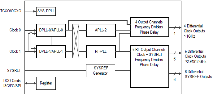
The 8V19N850 is a fully integrated Radio Unit Clock Synchronizer and Jitter Attenuator designed as a high-performance clock solution for phase/frequency synchronization and signal conditioning of wireless base station radio equipment. The device supports JESD204B/C subclass 0 and 1 device clocks and SYSREF synchronization for converters. The 8V19N850 supports two independent frequency domains: one that can be used for the digital clock (Ethernet and FEC rates) domain with four outputs, and the device clock (RF-PLL) domain with 12 outputs. The Ethernet domain generates frequencies from two independent APLLs for flexibility; the outputs of the RF clock domain generate very low phase noise clocks for ADC/DAC circuits.
From the integrated RF-PLL, the device supports the clock generation of high-frequency device clocks for driving ADC/DAC devices low-frequency synchronization signals (SYSREF). A dual DPLL front-end architecture supports any frequency translation. Each DPLL provides a programmable bandwidth and a DCO function for real-time frequency/phase adjustments. The DPLLs can lock on 1PPS input signals and establish lock within 100s or less. Frequency information can be applied from DPLL-0 to DPLL-1 and vice versa to enable the combining of the frequency characteristics of two references (combo-mode). The 8V19N850 is configured through a pin-mapped I3C (including legacy I2C) and 3/4-wire SPI interface. I2C with master capabilities reads a default configuration from an external ROM device. GPIO ports can be configured for reporting and controlling purposes.
Features
- Device clock domain (RF-PLL) with support for JESD204B/C
- Digital clock domain (Ethernet, FEC) with support for eEEC and T-BC/T-TSC Class C
- 2 differential clock reference inputs with 1PPS (1Hz) to 1GHz input frequency
- Dual DPLL front-end with independent clock paths
- External control of the DCO for IEEE1588
- Digital holdover with a 1.1 × 10⁻⁷ ppb accuracy
- Programmable DPLL loop bandwidth 1mHz - 6kHz
- Configurable phase delay (range: 1UI)
- Hitless input switching with < 1ns output phase error
- Reference monitors for input LOS, activity and frequency
- 1 external synchronization input for JESD204B/C (LVCMOS)
- 16 differential outputs
- Optimized for low phase noise: -146dBc/Hz (1MHz offset; 245.76MHz clock)
- Supply voltage (core): 3.3V; (outputs): 3.3V, 2.5V, and 1.8V
- Board temperature range: -40°C to +105°C
- Applicable Standards
- ITU-T G.8262 EEC1/2, G.8262.1 eEEC
- ITU-T G.8273.2 T-BC/T-TSC Class C
- JESD204B and C
Comparison
Applications
Design & Development
Software & Tools
Boards & Kits
Evaluation
8V19N850-EVK
Preview
8V19N850 Evaluation Kit
The evaluation kit supports electrical AC and DC measurements of the 8V19N850DNLGI, a fully integrated radio synchronizer and JESD204B/C clock jitter attenuator. The device on the board accepts any input frequency from 1Hz to 1GHz. Locked to a selected input, the device PLLs generate clock and...
Recommended Documents:
Models
ECAD Models
Schematic symbols, PCB footprints, and 3D CAD models from SamacSys can be found by clicking on the CAD Model links in the Product Options table. If a symbol or model isn't available, it can be requested directly from SamacSys.

Product Options
Applied Filters:
Videos & Training
8V19N850 5G Radio Synchronizer
This video introduces the industry’s first fully-integrated synchronizer for 5G enhanced common public radio interface (eCPRI) radio synchronization.
Video List

Demystifying 5G Video Series
Rohde & Schwarz's Demystifying 5G video series discusses main topics related to 5G including new technology components, procedures and testing challenges.
Events & Webinars

News & Blog Posts
Blog Post
Feb 1, 2022
|