Overview
Description
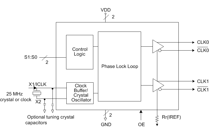
The IDT5V41315 is a PCIe Gen1/2/3 clock synthesizer suitable for use in both Common-Clocked and Separate Reference clock with No Spread (SRNS) timing architectures. The IDT5V41315 uses a 25MHz input to generate 4 different output frequencies. The output frequency is selectable via select pins.
Features
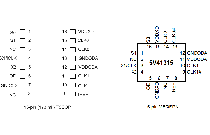
- 16-pin TSSOP or VFQFPN package; small board footprint
- Outputs can be terminated to LVDS; can drive a wider variety of devices
- OE control pin; greater system power management
- Industrial temperature range available; supports demanding embedded applications
- Cycle-to-cycle jitter: 80ps
- Output-to-output skew: <50 ps
- PCIe Gen2 phase jitter: <3.0ps RMS (Common Clock)
- PCIe Gen3 phase jitter: <1.0ps RMS (Common Clock)
- Low Phase Noise: 12KHz to 20MHz <6ps RMS
Comparison
Applications
Design & Development
Models
ECAD Models
Schematic symbols, PCB footprints, and 3D CAD models from SamacSys can be found by clicking on the CAD Model links in the Product Options table. If a symbol or model isn't available, it can be requested directly from SamacSys.

Product Options
Applied Filters:
Videos & Training
PCIe Clocking Architectures (Common and Separate)
This is the first video in our PCIe series. In this video, we define PCIe architectures, focusing on common and separate clock architectures. Watch the rest of the video series below where Ron will cover the impact of different timing architectures.
Watch the Video Series Below
Video List