Features
- DIF output cycle-to-cycle jitter < 50ps
- DIF output-to-output skew < 150 ps
- PCIe Gen2 compliant phase noise
- QPI 133MHz compliant phase noise
- Supports output clock frequencies up to 400 MHz
- 4 Selectable SMBus addresses
- SMBus address is independent of PLL operating mode
- Dedicated CKPWRGD/PD# and VDDA pins ease board design
- Available in industrial temperature range (-40°C to +85°C)
Description
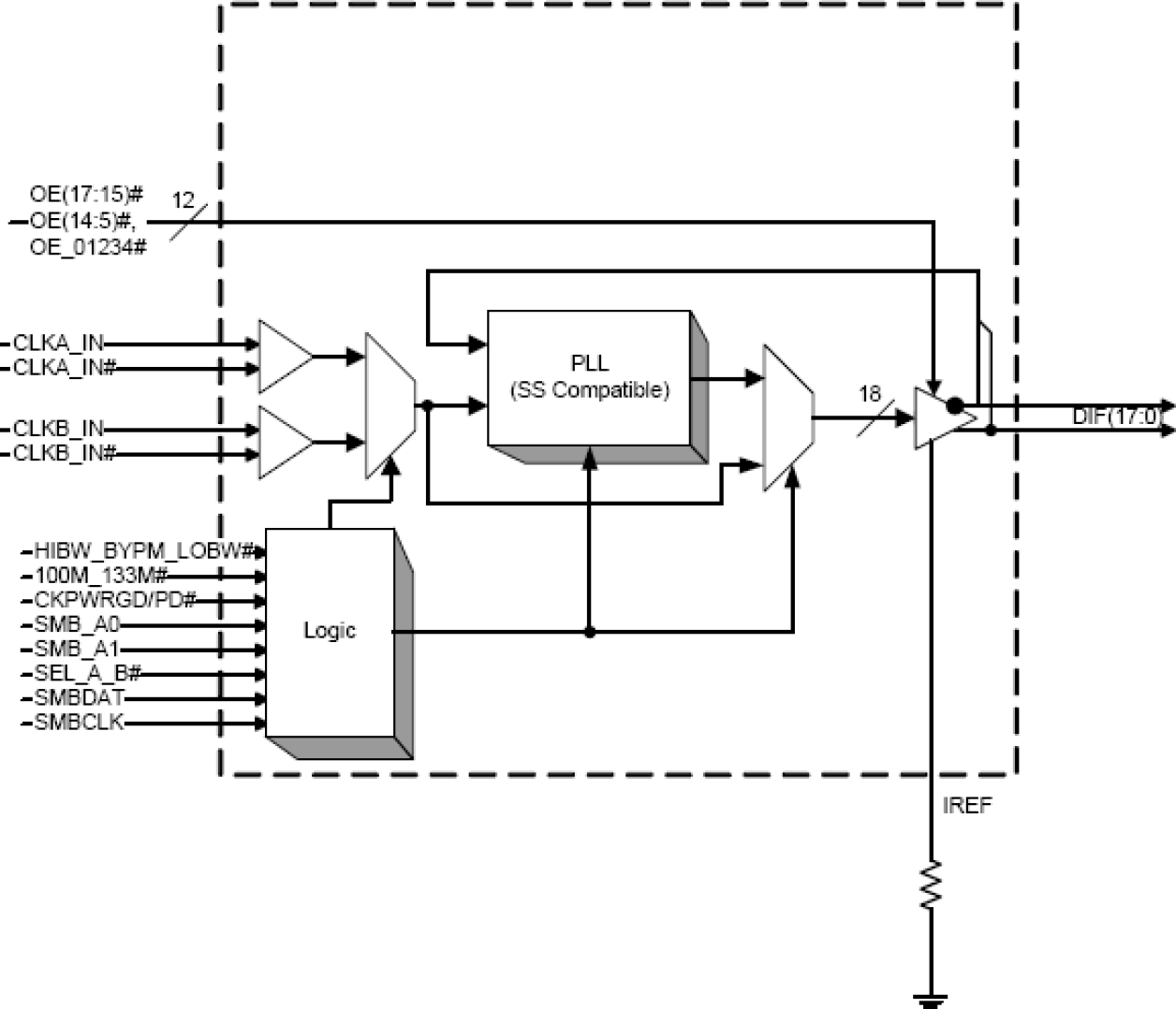
The 9EX21801 provides 18 output clocks for PCIe Gen2 (100MHz) or QPI (133MHz) applications. The 9EX21801 has 4 selectable SMBus addresses, and dedicated CKPWRGD/PD# and VDDA pins for easy board design. A differential CPU clock from a CK410B+ main clock generator, such as the 932S421, drives the 9EX21801. In fanout mode, the 9EX21801 provides outputs up to 400MHz.
Applied Filters:
Filters
Software & Tools
Sample Code
Simulation Models
This is the first video in our PCIe series. In this video, we define PCIe architectures, focusing on common and separate clock architectures. Watch the rest of the video series below where Ron will cover the impact of different timing architectures.
In this episode, Ron Wade from IDT (acquired by Renesas) explains PCIe common clocking and its impact on timing solutions. Learn about using a single clock source, fan-out buffers, and the considerations for spread spectrum and non-spread spectrum clocking in PCIe systems.
In this video, we explore PCIe with separate reference clocks and the effects of clock selection. Learn how separate reference clocks work and their impact on system performance and stability.
This video provides a high-level overview of Separate Reference Clock with Independent Spread (SRIS) architectures for PCI Express systems, additional performance requirements that this clocking architecture imposes on the reference clocks, and some system implications encountered trying to implement the architecture.